Features: • Rich instruction set
439 instructions
Transfer, rotate, increment/decrement, arithmetic operations, comparison, logic operations,mask operations, bit operations, ROM table reference, external memory transfer, stack operations, flag operations, branch, conditional branch, call/return, control.
• Rich selection of addressing modes
Indirect addressing of four data memory types, with current bank register, extra bank register, HL register and XY register.Data memory bank internal direct addressing mode.
• Processing speed
Two clocks per machine cycle, with most instructions executed in one machine cycle.
Minimum instruction execution time : 61 ms (@ 32.768 kHz system clock)
1 ms (@ 2 MHz system clock)
• Clock generation circuit
Low-speed clock : 32.768 kHz crystal oscillator
High-speed clock : 2 MHz (Max.) RC or ceramic oscillator select
• Program memory space
4K words
Basic instruction length is 16 bits/1 word
• Data memory space
384 nibbles
• External data memory space
64 Kbytes (expandable by using an I/O port)
• Stack level
Call stack level : 8 levels
Register stack level : 16 levels
• I/O ports
Input ports: Selectable as input with pull-up resistance/input with pull-down resistance/high-impedance input
Output ports: Selectable as P-channel open drain output/N-channel open drain output/CMOS output/high-impedance output
Input-output ports: Selectable as input with pull-up resistance/input with pull-down resistance/high-impedance input
Selectable as P-channel open drain output/N-channel open drain output/CMOS output/high-impedance output Can be interfaced with external peripherals that use a different power supply than this device uses.
Number of ports:
Input port : 2 ports × 4 bits
Output port : 4 ports × 4 bits
Input-output port : 3 ports × 4 bits
• Buzzer function
Buzzer output : 0.946 to 5.461 kHz (adjustable in 15 steps)
Buzzer output modes : Intermittent sound 1, 2; simple sound; continuous sound
• LCD driver
Number of segments : 512 Max. (32 SEG × 16 COM)
1/1 to 1/16 duty
1/4 or 1/5 bias (regulator built-in)
Selectable as all-on mode/all-off mode/power down mode/normal display mode Adjustable contrast
• Reset function
Reset through RESET pin
Power-on reset
Reset by low-speed oscillation halt
• Battery check
Low-voltage supply check
Criterion voltage : Can be selected as 1.05 ±0.10 V, 1.30 ±0.15 V,
2.20 ±0.20 V or 2.80 ±0.30 V
• Power supply backup
Backup circuit (voltage multiplier) enables operation at 0.9 V minimum
• Timers and counter
Watchdog timer × 1
Overflows in 2 sec.
100 Hz timer× 1
Measurable in steps of 1/100 sec.
15-bit time base counter ×1
1, 2, 4, 8, 16, 32, 64, and 128 Hz signals can be read
• Interrupt sources
External interrupt : 2
Internal interrupt : 6 (watchdog timer interrupt is a nonmaskable interrupt)
• Operating voltage
When backup used : 0.9 to 2.7 V
(Low-speed clock operating)
1.2 to 2.7 V
(Operating frequency: 300 to 500 kHz)
1.5 to 2.7 V
(Operating frequency: 200 kHz to 1 MHz)
When backup not used : 1.8 to 5.5 V
(Operating frequency: 300 to 500 kHz)
2.2 to 5.5 V
(Operating frequency: 300 kHz to 1 MHz)
2.7 to 5.5 V
(Operating frequency: 200 kHz to 2 MHz)
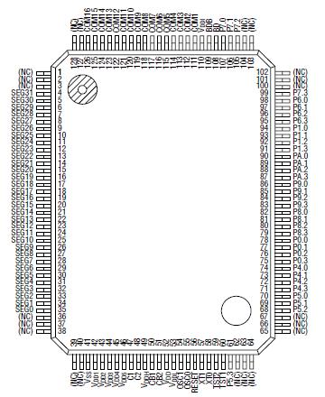
• Package:
128-pin plastic QFP (QFP128-P-1420-0.50-K) : (Product name: MSM63182-xxxGS-K)
Chip : (Product name: MSM63182-xxx)
xxx indicates a code number.
Pinout Specifications
|
Parameter |
Symbol |
Condition |
Rating |
Unit |
| Power Supply Voltage 1 |
VDD1 |
Ta = 25°C |
0.3 to +1.6 |
V |
| Power Supply Voltage 2 |
VDD2 |
Ta = 25°C |
0.3 to +2.9 |
| Power Supply Voltage 3 |
VDD3 |
Ta = 25°C |
0.3 to +4.2 |
| Power Supply Voltage 4 |
VDD4 |
Ta = 25°C |
0.3 to +5.5 |
| Power Supply Voltage 5 |
VDD5 |
Ta = 25°C |
0.3 to +6.8 |
| Power Supply Voltage 6 |
VDD |
Ta = 25°C |
0.3 to +6.0 |
| Power Supply Voltage 7 |
VDDI |
Ta = 25°C |
0.3 to +6.0 |
| Power Supply Voltage 8 |
VDDH |
Ta = 25°C |
0.3 to +6.0 |
| Power Supply Voltage 9 |
VDDL |
Ta = 25°C |
0.3 to +6.0 |
| Input Voltage 1 |
VIN1 |
VDD Input, Ta = 25°C |
0.3 to VDD + 0.3 |
| Input Voltage 2 |
VIN2 |
VDDI Input, Ta = 25°C |
0.3 to VDDI + 0.3 |
| Output Voltage 1 |
VOUT1 |
VDD1 Input, Ta = 25°C |
0.3 to VDD1 + 0.3 |
| Output Voltage 2 |
VOUT2 |
VDD2 Input, Ta = 25°C |
0.3 to VDD2 + 0.3 |
| Output Voltage 3 |
VOUT3 |
VDD3 Input, Ta = 25°C |
0.3 to VDD3 + 0.3 |
| Output Voltage 4 |
VOUT4 |
VDD4 Input, Ta = 25°C |
0.3 to VDD4 + 0.3 |
| Output Voltage 5 |
VOUT5 |
VDD5 Input, Ta = 25°C |
0.3 to VDD5 + 0.3 |
| Output Voltage 6 |
VOUT6 |
VDD Input, Ta = 25°C |
0.3 to VDD + 0.3 |
| Output Voltage 7 |
VOUT7 |
VDDI Input, Ta = 25°C |
0.3 to VDDI + 0.3 |
| Output Voltage 8 |
VOUT8 |
VDDH Input, Ta = 25°C |
0.3 to VDDH + 0.3 |
| Storage Temperature |
TSTG |
- |
55 to +150 |
°C |
DescriptionThe MSM63182 is a CMOS 4-bit microcontroller with built-in 512-dot matrix LCD drivers and operates at 0.9 V (min.).
The MSM63182 is suitable for applications such as games, toys, watches,etc. which are provided with an LCD display.
The MSM63182 is an M6318x series mask ROM-version product of OLMS-63K family, which employs Oki's original CPU core nX-4/250.
The MSM63P180 is the one-time-programmable ROM version of MSM63188, having one-time PROM (OTP) as internal program memory.
The MSM63P180 is used to evaluate the software development.

 MSM63182 Data Sheet


