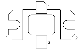
Features: · REFRACTORY/GOLD METALLIZATION· EMITTER SITE BALLASTED· LOW THERMAL RESISTANCE· INPUT/OUTPUT MATCHING· OVERLAY GEOMETRY· METAL/CERAMIC HERMETIC PACKAGE· POUT = 25 W MIN. WITH 7.0 dB GAINPinoutSpecifications Symbol Parameter Value Unit PDISS Power Dissipation* (TC ...
MS2620: Features: · REFRACTORY/GOLD METALLIZATION· EMITTER SITE BALLASTED· LOW THERMAL RESISTANCE· INPUT/OUTPUT MATCHING· OVERLAY GEOMETRY· METAL/CERAMIC HERMETIC PACKAGE· POUT = 25 W MIN. WITH 7.0 dB GAINP...
SeekIC Buyer Protection PLUS - newly updated for 2013!
268 Transactions
All payment methods are secure and covered by SeekIC Buyer Protection PLUS.
Symbol |
Parameter |
Value |
Unit |
PDISS |
Power Dissipation* (TC 75) |
500 |
W |
IC |
Device Current* |
16 |
A |
VCC |
Collector-Supply Voltage* |
45 |
V |
TJ |
Junction Temperature(Pulsed RF Operation) |
+200 |
|
TSTG |
Storage Temperature |
- 65 to + 200 |
The MS2620 device is a high power silicon bipolar NPN transistor specifically designed for medium pulse S-Band radar output and driver applications.
This MS2620 device is characterized at 50 sec pulse width and 10% duty cycle, but is cable of operation over a range of pulse widths, duty cycles and temperatures, and can withstand a 3:1 output VSWR with a + 1 dB input overdrive. Low RF thermal resistance, refractory/gold metallization and computerized automatic wire bonding techniques ensure high reliability and product consistancy (including phase characteristics).
The MS2620 is supplied in the BIGPACTM Hermetic Metal/Ceramic package with internal Input/Output impedance matching circuitry, and is intended for military and other high reliability applications.