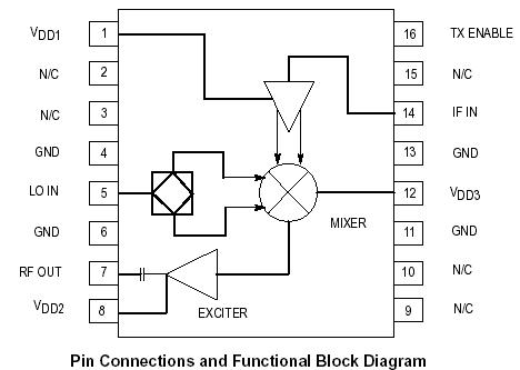
PinoutSpecifications Parameter Symbol Limit Units Supply Voltage VDD 5.5 Vdc RF Input Power PRF 3 dBm LO Input Power PLO 3 dBm Drain Current IDD 5.5 mA Storage Temperature Range Tstg 65 to+150 °C Operating ...
MRFIC1813: PinoutSpecifications Parameter Symbol Limit Units Supply Voltage VDD 5.5 Vdc RF Input Power PRF 3 dBm LO Input Power PLO 3 dBm Drain Cu...
SeekIC Buyer Protection PLUS - newly updated for 2013!
268 Transactions
All payment methods are secure and covered by SeekIC Buyer Protection PLUS.
Parameter |
Symbol |
Limit |
Units |
Supply Voltage |
VDD |
5.5 |
Vdc |
RF Input Power |
PRF |
3 |
dBm |
LO Input Power |
PLO |
3 |
dBm |
Drain Current |
IDD |
5.5 |
mA |
Storage Temperature Range |
Tstg |
65 to+150 |
°C |
Operating Ambient Temperature |
TA |
30 to +85 |
°C |
Designed primarily for use in wireless Personal Communication Systems PCS) applications such as Digital European Cordless Telephone (DECT), Japan's Personal Handy System (PHS) and the emerging North American systems. The MRFIC1813 is also applicable to 2.4 GHz ISM equipment. The device combines a balanced upmixer and a transmit exciter amplifier in a low-cost TSSOP16 package. Minimal off-chip matching is required while allowing for maximum flexibility and efficiency. The mixer is optimized for lowside injection and provides more than 12 dB of conversion gain with over 0 dBm output at 1 dB gain compression. Image filtering is implemented off-chip to allow maximum flexibility. A CMOS compatible ENABLE pin allows standby operation where the current drain is less than 250 A. Together with other devices from the MRFIC180X or the MRFIC240X series, this GaAs IC family offers the complete transmit and receive functions, less LO and filters, needed for a typical 1.8 GHz cordless telephone or 2.4 GHz ISM band equipment.