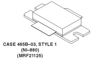
MRF21125

ApplicationTypical 2carrier WCDMA Performance for VDD = 28 Volts, IDQ = 1600mA, f1 = 2.1125 GHz, f2 = 2.1225 GHz, Channel bandwidth = 3.84 MHz,adjacent channels at ± 5 MHz , ACPR and IM3 measured in 3.84 MHzbandwidth. Peak/Avg = 8.5 dB @ 0.01% probability on CCDF.Output Power - 20 WattsEfficiency ...

product image

MRF21125 Picture
SeekIC No. : 004426925 Detail

MRF21125: ApplicationTypical 2carrier WCDMA Performance for VDD = 28 Volts, IDQ = 1600mA, f1 = 2.1125 GHz, f2 = 2.1225 GHz, Channel bandwidth = 3.84 MHz,adjacent channels at ± 5 MHz , ACPR and IM3 measured in...

floor Price/Ceiling Price

Part Number:
MRF21125
Supply Ability:
5000

Price Break

  • Qty
  • 1~5000
  • Unit Price
  • Negotiable
  • Processing time
  • 15 Days
Total Cost: $ 0.00

SeekIC Buyer Protection PLUS - newly updated for 2013!

  • Escrow Protection.
  • Guaranteed refunds.
  • Secure payments.
  • Learn more >>

Month Sales

268 Transactions

Rating

evaluate  (4.8 stars)

Upload time: 2024/11/26

Payment Methods

All payment methods are secure and covered by SeekIC Buyer Protection PLUS.

Notice: When you place an order, your payment is made to SeekIC and not to your seller. SeekIC only pays the seller after confirming you have received your order. We will also never share your payment details with your seller.
Product Details

Description


Application

Typical 2carrier WCDMA Performance for VDD = 28 Volts, IDQ = 1600
mA, f1 = 2.1125 GHz, f2 = 2.1225 GHz, Channel bandwidth = 3.84 MHz,
adjacent channels at ± 5 MHz , ACPR and IM3 measured in 3.84 MHz
bandwidth. Peak/Avg = 8.5 dB @ 0.01% probability on CCDF.
Output Power - 20 Watts
Efficiency - 18%
Gain - 13 dB
IM3 - 43 dBc
ACPR - 45 dBc
100% Tested under 2carrier WCDMA
Internally Matched, Controlled Q, for Ease of Use
High Gain, High Efficiency and High Linearity
Integrated ESD Protection
Designed for Maximum Gain and Insertion Phase Flatness
Capable of Handling 5:1 VSWR, @ 28 Vdc, 2170 MHz, 125 Watts (CW) Output Power
Excellent Thermal Stability
Characterized with Series Equivalent LargeSignal Impedance Parameters
Available in Tape and Reel. R3 Suffix = 250 Units per 56 mm, 13 inch Reel.


Pinout


Specifications

Rating Symbol Value Unit
Drain-Source Voltage VDSS 65 Vdc
Gate-Source Voltage VGS -0.5, +15 Vdc
Total Device Dissipation @ TC = 25°C
Derate above 25°C
PD 330
1.89
Watts
W/°C
Storage Temperature Range Tstg -65 to +150 °C
Operating Junction Temperature TJ 200 °C


Description

The MRF21125 is designed as RF power field effect transistors of N-channel enhancement-mode lateral MOSFETs for W-CDMA base station applications with frequencies from 2110 to 2170 MHz. Suitable for TDMA, CDMA and multicarrier amplifier applications. To be used in class AB for PCNPCS/cellular radio and WLL applications.

MRF21125 has ten features. (1) Typical 2carrier WCDMA Performance for VDD = 28Volts, IDQ = 1600mA, f1 = 2.1125 GHz, f2 = 2.1225GHz, channel bandwidth = 3.84MHz, adjacent channels at ±5MHz , ACPR and IM3 measured in 3.84MHz bandwidth. Peak/Avg = 8.5 dB @ 0.01% probability on CCDF. (2) 100% tested under 2carrier W-CDMA. (3) Internally matched, controlled Q, for ease of use. (4) High gain, high efficiency and high linearity. (5) Integrated ESD protection. (6) Designed for maximum gain and insertion phase flatness. (7) Capable of handling 5:1 VSWR, at 28Vdc, 2170MHz, 125Watts (CW) output power. (8) Excellent thermal stability. (9) Characterized with series equivalent large signal impedance parameters. (10) Available in tape and reel. R3 suffix = 250 units per 56mm, 13 inch reel. That are all the main features.

Some absolute maximum ratings of MRF21125 have been concluded into several points as follow. (1) Its drain to source voltage would be 65V. (2) Its gate to source voltage would be +15Vdc, -0.5Vdc. (3) Its total device dissipation would be 330W at 25°C and would be 1.89W/°C for derate above 25°C. (4) Its storage temperature range would be from -65°C to +150°C. (5) Its operating junction temperature would be 200°C.

Also some electrical characteristics about MRF21125. (1) Its drain to source breakdown voltage would be min 65V. (2) Its gate to source leakage current would be max 1uAdc. (3) Its zero gate voltage drain leakage current would be max 10uAdc. (4) Its forward transconductance would be typ 10.8S. (5) Its gate threshold voltage would be min 2Vdc and max 4Vdc. And so on. If you have any question or suggestion or want to know more information please contact us for details. Thank you!


Customers Who Bought This Item Also Bought

Margin,quality,low-cost products with low minimum orders. Secure your online payments with SeekIC Buyer Protection.
Cables, Wires
Industrial Controls, Meters
Hardware, Fasteners, Accessories
Optical Inspection Equipment
Prototyping Products
DE1
LED Products
View more