MPC9992

Features: • 7 differential outputs, PLL based clock generator• SiGe technology supports minimum output skew (max. 150 ps1)• Supports up to two generated output clock frequencies with a maximum clock frequency up to 400 MHz• Selectable crystal oscillator interface and PECL c...

product image

MPC9992 Picture
SeekIC No. : 004426210 Detail

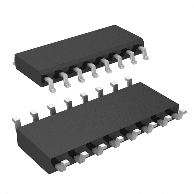
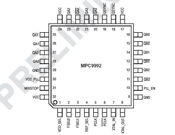
MPC9992: Features: • 7 differential outputs, PLL based clock generator• SiGe technology supports minimum output skew (max. 150 ps1)• Supports up to two generated output clock frequencies wi...

floor Price/Ceiling Price
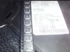
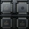
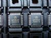
Part Number:
MPC9992
Supply Ability:
5000

Price Break

  • Qty
  • 1~5000
  • Unit Price
  • Negotiable
  • Processing time
  • 15 Days
Total Cost: $ 0.00

SeekIC Buyer Protection PLUS - newly updated for 2013!

  • Escrow Protection.
  • Guaranteed refunds.
  • Secure payments.
  • Learn more >>

Month Sales

268 Transactions

Rating

evaluate  (4.8 stars)

Upload time: 2024/6/27

Payment Methods

All payment methods are secure and covered by SeekIC Buyer Protection PLUS.

Notice: When you place an order, your payment is made to SeekIC and not to your seller. SeekIC only pays the seller after confirming you have received your order. We will also never share your payment details with your seller.
Product Details

Description


Features:

• 7 differential outputs, PLL based clock generator
• SiGe technology supports minimum output skew (max. 150 ps1)
• Supports up to two generated output clock frequencies with a maximum clock frequency up to 400 MHz
• Selectable crystal oscillator interface and PECL compatible clock input
• SYNC pulse generation
• PECL compatible differential clock inputs and outputs
• Single 3.3V (PECL) supply
• Ambient temperature range 0 to +70
• Standard 32 lead LQFP package
• Pin and function compatible to the MPC992


Application

The MPC9992 has a system synchronization pulse output QSYNC. In configurations with the output frequency relationships are not integer multiples of each other QSYNC provides a signal for system synchronization purposes. The MPC9992 monitors the relationship between the A bank and the B bank of outputs. The QSYNC output is asserted (logichigh) one QA period in duration after the coincident rising edges of the QA and QB outputs. The placement of the pulse is dependent on the QA and QB output frequencies ratio. Table 2 shows the waveforms for the QSYNC output. The QSYNC output is defined for all possible combinations of the bank A and bank B outputs.


Pinout

  Connection Diagram


Specifications

Symbol Characteristics Min Max Unit Condition
VCC Supply Voltage -0.3 3.6 V  
VIN DC Input Voltage -0.3 VCC+0.3 V  
VOUT DC Output Voltage -0.3 VCC+0.3 V  
IIN DC Input Current   ±20 mA  
IOUT DC Output Current   ±50 mA  
TS Storage Temperature -65 125  


Description

The MPC9992 utilizes PLL technology to frequency lock its outputs onto an input reference clock. The reference clock frequency and the divider for the feedback path determine the VCO frequency. Both must be selected to match the VCO frequency range. The MPC9992 features frequency programmability between the three output banks outputs as well as the output to input relationships. Output frequency ratios of 2:1, 3:1, 3:2 and 5:2 can be realized. The two banks of outputs and the feedback frequency divider can be programmed by the FSEL[2:0] pins of the MPC9992. The VCO_SEL pin provides an extended PLL input reference frequency range.

The SYNC pulse generator monitors the phase relationship between the QA[3:0] and QB[2:0] output banks. The SYNC generator output signals the coincident edges of the two output banks. MPC9992 feature is useful for non binary relationships between output frequencies.

The REF_SEL pin selects the differential PECL compatible input pair or crystal oscillator interface of MPC9992 as the reference clock signal. The PLL_EN control selects the PLL bypass configuration for test and diagnosis. In this configuration, the selected input reference clock is routed directly to the output dividers bypassing the PLL. The PLL bypass is fully static and the minimum clock frequency specification and all other PLL characteristics do not apply.

The MPC9992 requires an external reset signal for start-up and for PLL recovery in case the reference input is interrupted. Assertion of the reset signal forces all outputs to the logic low state.

The MPC9992 is fully 3.3V compatible and requires no external loop filter components. The differential clock input (PCLK) is PECL compatible and all control inputs accept LVCMOS compatible signals while the outputs provide PECL compatible levels with the capability to drive terminated 50 transmission lines.

The MPC9992 is pin and function compatible to the MPC992 and is packaged in a 32-lead LQFP package. 1. Final specification of this parameter is pending characterization.


Customers Who Bought This Item Also Bought

Margin,quality,low-cost products with low minimum orders. Secure your online payments with SeekIC Buyer Protection.
Inductors, Coils, Chokes
Programmers, Development Systems
Crystals and Oscillators
Discrete Semiconductor Products
Audio Products
Industrial Controls, Meters
View more