Features: • 12 output LVCMOS PLL clock generator• 2.5V and 3.3V compatible• IDCS - on-chip intelligent dynamic clock switch• Automatically detects clock failure• Smooth output phase transition during clock failover switch• 6.25 - 200 MHz output frequency range...
MPC9893: Features: • 12 output LVCMOS PLL clock generator• 2.5V and 3.3V compatible• IDCS - on-chip intelligent dynamic clock switch• Automatically detects clock failure• Smooth...
SeekIC Buyer Protection PLUS - newly updated for 2013!
268 Transactions
All payment methods are secure and covered by SeekIC Buyer Protection PLUS.
Symbol | Characteristics | Min | Max | Unit | Condition |
VCC | Supply Voltage | -0.3 | 3.6 | V | |
VIN | DC Input Voltage | -0.3 | VCC+0.3 | V | |
VOUT | DC Output Voltage | -0.3 | VCC+0.3 | V | |
IIN | DC Input Current | ±20 | mA | ||
IOUT | DC Output Current | ±50 | mA | ||
TS | Storage Temperature | -65 | 125 |
a. Absolute maximum continuous ratings are those maximum values beyond which damage to the device may occur. Exposure to these conditions or conditions beyond those indicated may adversely affect device reliability. Functional operation at absolute-maximum-rated conditions is not implied.
The MPC9893 is a 3.3V or 2.5V compatible PLL clock driver and clock generator. The clock generator uses a fully integrated PLL to generate clock signals from redundant clock sources. The PLL multiplies the input reference clock signal by one, two, three, four or eight. The frequency-multiplied clock drives six bank A outputs. Six bank B outputs can run at either the same frequency than bank A or at half of the bank A frequency. Therefore, bank B outputs additionally support the frequency multiplication of the input reference clock by 3÷2 and 1÷2. Bank A and bank B outputs are phase-aligned2. Due to the external PLL feedback, the clock signals of both output banks are also phase-aligned2 to the selected input reference clock, providing virtually zero-delay capability. The integrated IDCS continuously monitors both clock inputs and indicates a clock failure individually for each clock input. When a false clock signal is detected, the MPC9893 switches to the redundant clock input, forcing the PLL to slowly slew to alignment and not produce any phase bumps at the outputs. Both clock inputs are interchangeable, also supporting the switch to a failed clock that was restored. The MPC9893 also provides a manual mode that allows for user-controlled clock switches.
The PLL bypass of the MPC9893 disables the IDCS and PLL-related specifications do not apply. In PLL bypass mode, it is fully static in order to distribute low-frequency clocks for system test and diagnosis. Outputs of the MPC9893 can be disabled (high-impedance tristate) to isolate the device from the system. Applying output disable also resets the MPC9893. On power-up this reset function needs to be applied for correct operation of the circuitry. Please see the application section for power-on sequence recommendations.
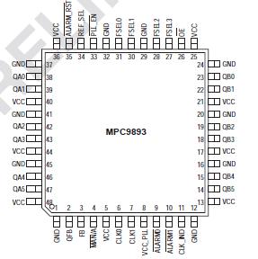
The MPC9893 is packaged in a 7x7 mm2 48-lead LQFP package.