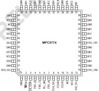
Features: • 1:14 PLL based low-voltage clock generator• 2.5V or 3.3V power supply• Internal poweron reset• Generates clock signals up to 125 MHz• Maximum output skew of 300 ps1• Two LVCMOS PLL reference clock inputs• External PLL feedback supports zero-del...
MPC9774: Features: • 1:14 PLL based low-voltage clock generator• 2.5V or 3.3V power supply• Internal poweron reset• Generates clock signals up to 125 MHz• Maximum output skew of...
SeekIC Buyer Protection PLUS - newly updated for 2013!
268 Transactions
All payment methods are secure and covered by SeekIC Buyer Protection PLUS.
Symbol | Characteristics | Min | Max | Unit | Condition |
VCC | Supply Voltage | -0.3 | 3.6 | V | |
VIN | DC Input Voltage | -0.3 | VCC+0.3 | V | |
VOUT | DC Output Voltage | -0.3 | VCC+0.3 | V | |
IIN | DC Input Current | ±20 | mA | ||
IOUT | DC Output Current | ±50 | mA | ||
TS | Storage Temperature | -65 | 125 |
a. Absolute maximum continuous ratings are those maximum values beyond which damage to the device may occur. Exposure to these conditions or conditions beyond those indicated may adversely affect device reliability. Functional operation at absolute-maximum-rated conditions is not implied.
The MPC9774 utilizes PLL technology to frequency lock its outputs onto an input reference clock. Normal operation of the MPC9774 requires the connection of the PLL feedback output QFB to feedback input FB_IN to close the PLL feedback path. The reference clock frequency and the divider for the feedback path determine the VCO frequency. Both must be selected to match the VCO frequency range.
The MPC9774 features frequency programmability between the three output banks outputs as well as the output to input relationships. Output frequency ratios of 1:1, 2:1, 3:1, 3:2 and 3:2:1 can be realized. Additionally, the MPC9774 supports a separate configurable feedback output which allows for a wide variety of of input/output frequency multiplication alternatives. The VCO_SEL pin provides an extended PLL input reference frequency range.
The REF_SEL pin selects the internal crystal oscillator or the LVCMOS compatible inputs as the reference clock signal. Two alternative LVCMOS compatible clock inputs of MPC9774 are provided for clock redundancy support. The PLL_EN control selects the PLL bypass configuration for test and diagnosis. In this configuration, the selected input reference clock is routed directly to the output dividers bypassing the PLL. The PLL bypass of MPC9774 is fully static and the minimum clock frequency specification and all other PLL characteristics do not apply.
The MPC9774 has an internal poweron reset.
The MPC9774 is fully 2.5V and 3.3V compatible and requires no external loop filter components. All inputs (except XTAL) accept LVCMOS signals while the outputs provide LVCMOS compatible levels with the capability to drive terminated 50 W transmission lines. For series terminated transmission lines, each of the MPC9774 outputs can drive one or two traces giving the devices an effective fanout of 1:12. The device is pin and function compatible to the MPC974 and is packaged in a 52-lead LQFP package.