Features: • 1:10 outputs LVCMOS zero-delay buffer• Single 3.3V or 2.5V supply• 150 ps maximum output skew1• ±100 ps static phase offset (SPO)1• Supports a clock I/O frequency range of 12.5 to 200 MHz• Selectable divide-by-two for one output bank• Synchrono...
MPC9608: Features: • 1:10 outputs LVCMOS zero-delay buffer• Single 3.3V or 2.5V supply• 150 ps maximum output skew1• ±100 ps static phase offset (SPO)1• Supports a clock I/O fre...
SeekIC Buyer Protection PLUS - newly updated for 2013!
268 Transactions
All payment methods are secure and covered by SeekIC Buyer Protection PLUS.
Symbol | Characteristics | Min | Max | Unit | Condition |
VCC | Supply Voltage | -0.3 | 3.6 | V | |
VIN | DC Input Voltage | -0.3 | VCC+0.3 | V | |
VOUT | DC Output Voltage | -0.3 | VCC+0.3 | V | |
IIN | DC Input Current | ±20 | mA | ||
IOUT | DC Output Current | ±50 | mA | ||
TS | Storage Temperature | -65 | 125 |
a. Absolute maximum continuos ratings are those maximum values beyond which damage to the device may occur. Exposure to these conditions or conditions beyond those indicated may adversely affect device reliability. Functional operation at absolute-maximum-rated conditions is not implied.
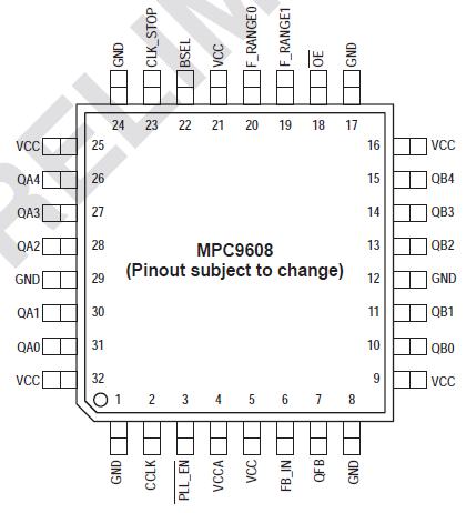
The MPC9608 uses an internal PLL and an external feedback path to lock its low-skew clock output phase to the reference clock phase, providing virtually zero propagation delay. This enables nested clock designs with near-zero insertion delay. Designs using the MPC9608 as PLL fanout buffer will show significantly lower clock skew than clock distributions developed from traditional fanout buffers. The MPC9608 offers one reference clock input and two banks of 5 outputs for clock fanout. The input frequency and phase is reproduced by the PLL and provided at the outputs. A selectable frequency divider sets the bank B outputs to generate either an identical copy of the bank A clocks or one half of the bank A clock frequency. Both output banks remain synchronized to the input reference for both bank B configurations.
Outputs of MPC9608 are only disabled or enabled when the outputs are already in logic low state (CLK_STOP). For system test and diagnosis, the MPC9608 outputs can also be set to high-impedance state by connecting OE to logic high level. Additionally, the device provides a PLL bypass mode for low frequency test purpose. In PLL bypass mode, the minimum frequency and static phase offset specification do not apply.
CLK_STOP and OE do not affect the PLL feedback output (QFB) and down stream clocks of MPC9608 can be disabled without the internal PLL losing lock.
The MPC9608 is fully 2.5V or 3.3V compatible and requires no external components for the internal PLL. All inputs accept LVCMOS signals while the outputs provide LVCMOS compatible levels with the capability to drive terminated 50 W transmission lines on the incident edge. For series terminated transmission lines, each of the MPC9608 outputs can drive one or two traces giving the devices an effective fanout of 1:20. The device is packaged in a 7x7 mm2 32-lead LQFP package.