Features: • 9 outputs LVCMOS PLL clock generator
• 25 - 240 MHz output frequency range
• Fully integrated PLL
• Compatible to various microprocessors such as PowerQuicc II
• Supports networking, telecommunications and computer applications
• Configurable outputs: divide-by-2, 4 and 8 of VCO frequency
• LVPECL and LVCMOS compatible inputs
• External feedback enables zero-delay configurations
• Output enable/disable and static test mode (PLL enable/disable)
• Low skew characteristics: maximum 150 ps output-to-output
• Cycle-to-cycle jitter max. 22 ps RMS
• 32 lead LQFP package
• Ambient Temperature Range 0°C to +70°C
• Pin & Function Compatible with the MPC951ApplicationThe fully integrated PLL of the MPC93R51 allows the low skew outputs to lock onto a clock input and distribute it with essentially zero propagation delay to multiple components on the board. In zero-delay buffer mode, the PLL minimizes phase offset between the outputs and the reference signal.
Pinout Specifications
| Symbol |
Characteristics |
Min |
Max |
Unit |
Condition |
| VCC |
Supply Voltage |
-0.3 |
4.6 |
V |
|
| VIN |
DC Input Voltage |
-0.3 |
VCC + 0.3 |
V |
|
| VOUT |
DC Output Voltage |
-0.3 |
VCC + 0.3 |
V |
|
| IIN |
DC Input Current |
|
±20 |
mA |
|
| IOUT |
DC Output Current |
|
±50 |
mA |
|
| TS |
Storage Temperature |
-55 |
150 |
°C |
|
a. Absolute maximum continuos ratings are those maximum values beyond which damage to the device may occur.
Exposure to these conditions or conditions beyond those indicated may adversely affect device reliability. Functional
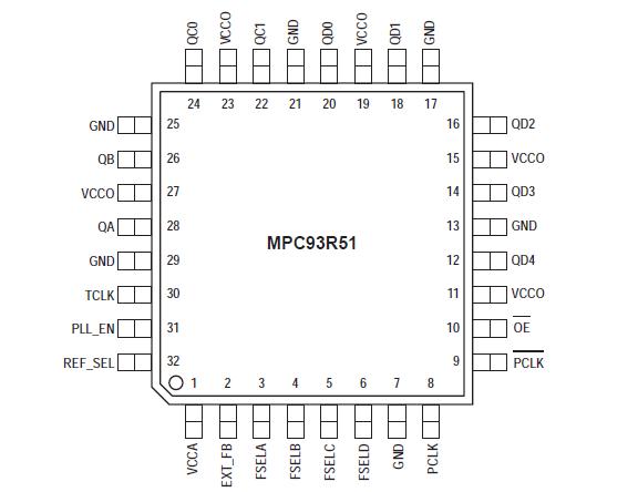
operation at absolute-maximum-rated conditions is not implied.DescriptionThe MPC93R51 utilizes PLL technology to frequency and phase lock its outputs onto an input reference clock. Normal operation of the MPC93R51 requires a connection of one of the device outputs to the EXT_FB input to close the PLL feedback path. The reference clock frequency and the output divider for the feedback path determine the VCO frequency. Both must be selected to match the VCO frequency range. With available output dividers of divide-by-4 and divide-by-8 the internal VCO of the MPC93R51 is running at either 4x or 8x of the reference clock frequency. The frequency of the QA, QB, QC and QD outputs is either the one half, one fourth or one eighth of the selected VCO frequency and can be configured for each output bank using the FSELA, FSELB, FSELC and FSELD pins, respectively. The available output to input frequency ratios are 4:1, 2:1, 1:1, 1:2 and 1:4. The REF_SEL pin selects the differential LVPECL (PCLK and PCLK) or the LVCMOS compatible reference input (TCLK). The MPC93R51 also provides a static test mode when the PLL enable pin (PLL_EN) is pulled to logic low state. In test mode, the selected input reference clock is routed directly to the output dividers bypassing the PLL. The test mode is intended for system diagnostics, test and debug purpose. This test mode is fully static and the minimum clock frequency specification does not apply. The outputs can be disabled by deasserting the OE pin (logic high state). In PLL mode, deasserting OE causes the PLL to loose lock due to no feedback signal presence at EXT_FB. AssertingOE will enable the outputs and close the phase locked loop, also enabling the PLL to recover to normal operation. The MPC93R51 is 3.3V compatible and requires no external loop filter components. All inputs except PCLK and PCLK accept LVCMOS signals while the outputs provide LVCMOS compatible levels with the capability to drive terminated 50 transmission lines. For series terminated transmission lines, each of the MPC93R51 outputs can drive one or two traces giving the devices an effective fanout of 1:18. The device is packaged in a 7x7 mm2 32-lead LQFP package.

 MPC93R51 Data Sheet


