Features: • 9 outputs LVCMOS PLL clock generator• 25 200 MHz output frequency range• 2.5V and 3.3V compatible• Compatible to various microprocessor such as PowerQuicc II• Supports networking, telecommunications and computer applications• Fully integrated PLL...
MPC9350: Features: • 9 outputs LVCMOS PLL clock generator• 25 200 MHz output frequency range• 2.5V and 3.3V compatible• Compatible to various microprocessor such as PowerQuicc IIR...
SeekIC Buyer Protection PLUS - newly updated for 2013!
268 Transactions
All payment methods are secure and covered by SeekIC Buyer Protection PLUS.
Symbol | Characteristics | Min | Max | Unit | Condition |
VCC | Supply Voltage | -0.3 | 4.6 | V | |
VIN | DC Input Voltage | -0.3 | VCC + 0.3 | V | |
VOUT | DC Output Voltage | -0.3 | VCC + 0.3 | V | |
IIN | DC Input Current | ±20 | mA | ||
IOUT | DC Output Current | ±50 | mA | ||
TS | Storage Temperature | -40 | 125 | °C |
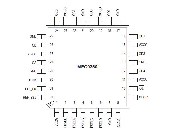
The MPC9350 generates high frequency clock signals and provides nine exact frequency-multiplied copies of the reference clock signal. The internal PLL allows the MPC9350 to operate in frequency locked condition and to multiply the input reference clock. The reference clock frequency and the divider in the internal feedback path determine the VCO frequency. Two selectable PLL feedback frequency ratios are available on the MPC9350 to provide input frequency range flexibility. The FBSEL pin selects between divide-by-16 or divide-by-32 of the VCO frequency for PLL feedback. This feedback divider must be selected to match the VCO frequency range. With the available feedback output dividers the internal VCO of the MPC9350 is running at either 16x or 32x of the reference clock frequency. The frequency of the QA, QB, QC and QD outputs is either one half, one fourth or one eighth of the selected VCO frequency and can be configured for each output bank using the FSELA, FSELB, FSELC and FSELD pins, respectively. The available output to input frequency ratios are 16:1, 8:1, 4:1 and 2:1. The REF_SEL pin selects the crystal oscillator inputs or the LVCMOS compatible reference input (TCLK). TCLK also provides an external test clock in static test mode when the PLL enable pin (PLL_EN) is pulled to logic low state. In test mode, the selected input reference clock is routed directly to the output dividers without using the PLL. The test mode is intended for system diagnostics, test and debug purpose. This test mode is fully static and the minimum clock frequency specification does not apply. The outputs can be disabled by deasserting the OE pin (logic high state). In PLL mode, deasserting OE maintains PLL lock due to the internal feedback path. The MPC9350 is fully 2.5V and 3.3V compatible and requires no external loop filter components. The on-chip crystal oscillator requires no external components beyond a series resonant crystal. All inputs except the crystal oscillator interface accept LVCMOS signals while the outputs provide LVCMOS compatible levels with the capability to drive terminated 50 transmission lines. For series terminated transmission lines, each of the MPC9350 outputs can drive one or two traces giving the devices an effective fanout of 1:18. The device is packaged in a 7x7 mm2 32-lead LQFP package.