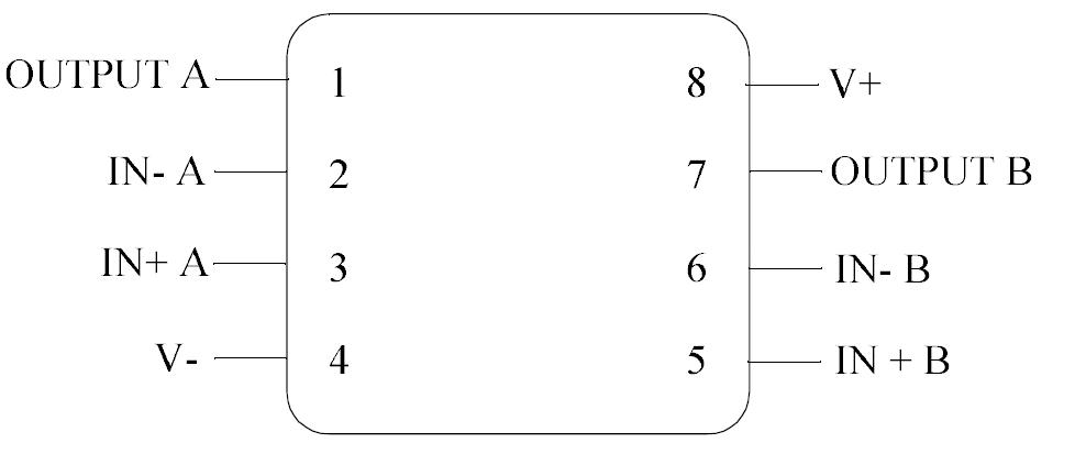
Features: ·Internally trimmed offset voltage. 1mV (max)
· Input offset voltage drift. 10uV/ C (max)
· Low input bias current. 50pA
·Low input noise current. 0.01 pA/Root Hz
·Wide gain bandwidth. 3MHz (min)
· High slew rate. 10V/uS (min)
· Low supply current. 1.8 mA/Amplifier
· High input impedance. 10E12 Ohms
· Low total harmonic distortion Av=10, RL=10K, +0.02% Vo = 20 Vp-p, BW = 20 Hz - 20KHz
· Low 1/f noise corner. 50Hz
· Fast settling time to 0.01%. 2uSPinout Specifications
Supply Voltage.............................................................+18V
Differential Input Voltage.............................................+30V
Input Voltage Range
(Note 3).......................................................................+15V
Output Short Circuit Duration
(Note 4).............................................................Continuous
Power Dissipation
(Note 2)
H Package ..............................................................800mW
(Note 3)
J Package ....................................................................TBD
Tjmax........................................................................150 C
ThetaJA (Typical)
METAL CAN
(Still Air) ...............................................................160 C/W
(500 LF/Min Air Flow)............................................. 83 C/W
CERDIP
(Still Air) .............................................................. 122 C/W
(500 LF/Min Air Flow) .............................................66 C/W
ThetaJC
METAL CAN............................................................ 38 C/W
CERDIP ..................................................................15 C/W
Operating Temperature Range.........-55 C TA 125 C
Storage Temperature Range............-65 C TA 150 C
Lead Temperature
Soldering, (10 Sec.) .................................................260 C
ESD Tolerance
(Note 5)...................................................................1700V
Note 1: Absolute Maximum Ratings indicate limits beyond
which damage to the device may occur. Operating Ratings
indicate conditions for which the device is functional, but
do not guarantee specific performance limits. For guaranteed
specifications and test conditions, see the Electrical
Characteristics. The guaranteed specifications applyonly for
the test conditions listed. Some performance characteristics
may degrade when the device is not operated under the
listed test conditions.
Note 2: The maximum power dissipation must be derated at
elevated temperatures and is dictated by Tjmax (maximum
junction temperature), ThetaJA (package junction to ambient
thermal resistance), and TA (ambient temperature). The
maximum allowable power dissipation at any temperature is
Pdmax = (Tjmax - TA)/ThetaJA or the number given in the
Absolute Maximum Ratings, whichever is lower.
Note 3: Unless otherwise specified the absolute maximum
negative input voltage is equal to the negative power supply
voltage.
Note 4: Any of the amplifier outputs can be shorted to ground
indefintely, however, more than one should not be simultane
ously shorted as the maximum junction temperature will be
exceeded.
Note 5: Human body model, 1.5K Ohms in series with 100pF.
DescriptionThese MNLF412-X devices are low cost, high speed, JFET input operational amplifiers with very low input offset voltage and guaranteed input offset voltage drift. They require low supply current yet maintain a large gain bandwidth product and fast slew rate. In addition, well matched high voltage JFET input devices provide very low input bias and offset currents. LF412 dual is pin compatible with the LM1558, allowing designers to immediately upgrade the overall performance of existing designs.
These MNLF412-X amplifiers may be used in applications such as high speed integrators,fast D/A converters, sample and hold circuits and many other circuits requiring low input offset voltage and drift, low input bias current, high input Impedance, high slew rate and wide bandwidth.

 MNLF412-X Data Sheet


