MNCLC522A-X

Features: ·330MHz signal bandwidth: Avmax = 2·165MHz gain-control bandwidth·0.3 degrees to 60MHz linear phase deviation·0.04% (-68dB) signal-channel non-linearity·>40dB gain-adjustment range·Differential or single-end voltage inputs·Single-ended voltage ouputApplication·Variable attenuators·Pul...

product image

MNCLC522A-X Picture
SeekIC No. : 004424753 Detail

MNCLC522A-X: Features: ·330MHz signal bandwidth: Avmax = 2·165MHz gain-control bandwidth·0.3 degrees to 60MHz linear phase deviation·0.04% (-68dB) signal-channel non-linearity·>40dB gain-adjustment range·Diff...

floor Price/Ceiling Price

Part Number:
MNCLC522A-X
Supply Ability:
5000

Price Break

  • Qty
  • 1~5000
  • Unit Price
  • Negotiable
  • Processing time
  • 15 Days
Total Cost: $ 0.00

SeekIC Buyer Protection PLUS - newly updated for 2013!

  • Escrow Protection.
  • Guaranteed refunds.
  • Secure payments.
  • Learn more >>

Month Sales

268 Transactions

Rating

evaluate  (4.8 stars)

Upload time: 2024/11/26

Payment Methods

All payment methods are secure and covered by SeekIC Buyer Protection PLUS.

Notice: When you place an order, your payment is made to SeekIC and not to your seller. SeekIC only pays the seller after confirming you have received your order. We will also never share your payment details with your seller.
Product Details

Description


Features:

· 330MHz signal bandwidth: Avmax = 2
· 165MHz gain-control bandwidth
· 0.3 degrees to 60MHz linear phase deviation
· 0.04% (-68dB) signal-channel non-linearity
· >40dB gain-adjustment range
· Differential or single-end voltage inputs
· Single-ended voltage ouput


Application

· Variable attenuators
· Pulse amplitude equalizers
· HF modulators
· Automatic gain control & leveling loops
· Video production switching
· Differential line receivers
· Voltage controlled filters


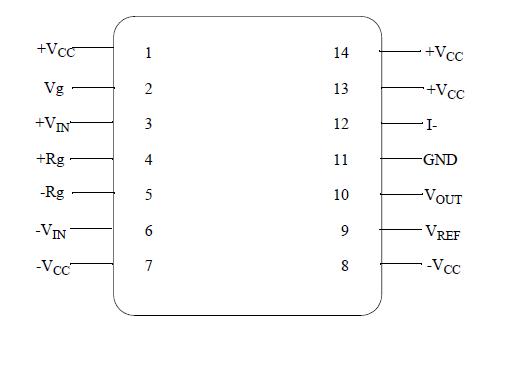
Pinout

  Connection Diagram


Specifications

Supply Voltage (Vs).............................................+7V dc
Output Current (Iout)...........................................95mA
Common Mode Input Voltage (Vcm)...........................Vs
Differential Input Voltage (Vid)..............................+10V
Power Dissipation (Pd)
(Note 2).............................................................810mW
Lead Temperature (soldering, 10 seconds).......+300 C
Junction Temperature (Tj)..................................+175 C
Storage Temperature Range................-65 C to +150 C
Thermal Resistance
Junction-to-Ambient (ThetaJA)
Ceramic DIP (Still Air) ........................................84 C/W
(500 LFPM) ........................................................44 C/W
LCC (Still Air) .....................................................85 C/W
(500 LFPM) ........................................................61 C/W
Junction-to-Case (ThetaJC)
Ceramic DIP ......................................................13 C/W
LCC ...................................................................21 C/W
Package Weight
(typical)
Ceramic DIP ...........................................................TBD
LCC ..................................................................470 mg
ESD Tolerance
(Note 3)
ESD Rating .........................................................500 V
Note 1: Absolute Maximum Ratings are limits beyond which damage to the device may occur. Operating Ratings are conditions for which the device is functional, but do not guarantee specific performance limits. For guaranteed specifications and test conditions see the Electrical Characteristics. The guaranteed specifications apply only for the test conditions listed. Some performance characteristics may degrade when the device is not operated under the listed test conditions.
Note 2: The maximum power dissipation must be derated at elevated temperatures and is dictated by Tjmax (maximum junction temperature), ThetaJA (package junction to ambient thermal resistance), and TA (ambient temperature). The maximum allowable power dissipation at any temperature is Pdmax = (Tjmax - TA)/ThetaJA or the number given in the Absolute Maximum Ratings, whichever is lower.
Note 3: Human body model, 100pF discharged through 1.5K Ohms.


Description

The CLC522 variable gain amplifier (VGA) is a dc-coupled, two-quadrant multiplier with differential voltage inputs and a single-ended voltage output. Two input buffers and an output operational amplifer are integrated with the multiplier core to make the CLC522 a complete VGA system that does not require external buffering.

The CLC522 provides the flexibility of externally setting the maximum gain with only two external resistors. Greater than 40dB gain control is easily achieved through a single high impedance voltage input. The CLC522 provides a linear (in Volts per Volt) relationship between the amplifier's gain and the gain-control input voltage.

The CLC522's maximum gain may be set anywhere over a nominal range of 2V/V to 100V/V. The gain control input then provides attenuation from the maximum setting. For example, set for a maximum gain of 100V/V, the CLC522 will provide a 100V/V to 1V/V gain control range by sweeping the gain control input voltage from +1 to -0.98V.

Set a maximum gain of 10V/V, the CLC522 provides a 165MHz signal channel bandwidth and a 165MHz gain control bandwidth. Gain non-linearity over a 40dB gain range is 0.5% and gain accuracy at Avmax = 10V/V is typically +0.3%.


Customers Who Bought This Item Also Bought

Margin,quality,low-cost products with low minimum orders. Secure your online payments with SeekIC Buyer Protection.
Power Supplies - External/Internal (Off-Board)
LED Products
Sensors, Transducers
Undefined Category
Optoelectronics
Industrial Controls, Meters
View more