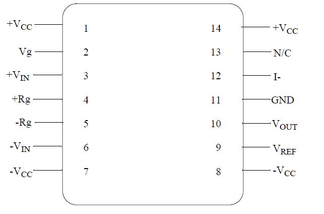
Features: · 160MHz, -3dB bandwidth
· 2000V/usec slew rate
· 0.04% signal nonlinearity at 4Vpp output
· -43dB feedthrough at 30MHz
· User adjustable gain range
· Differential voltage input and single-ended voltage outputApplication· Wide-bandwidth AGC systems
· Automatic signal-leveling
· Video signal processing
· Voltage controlled filters
· Differential amplifier
· Amplitude modulationPinout Specifications
Supply Voltage (V+)............................................+7V dc
Output Current (Iout)...........................................70mA
Common Mode Input Voltage (Vcm)..........................V+
Differential Input Voltage........................................10V
Gain Controlled Input Voltage..................................V+
Referenced Input Voltage (Vref)...............................V+
Maximum Power Dissipation (Pd)
(Note 2)................................................................1.2W
Junction Temperature (Tj).................................+175 C
Storage Temperature Range...............-65 C to +150 C
Lead Temperature (soldering, 10 seconds)......+300 C
Thermal Resistance
Junction -to-ambient (ThetaJA)
Ceramic DIP (Still Air) ......................................98 C/W
(500 LFPM) ......................................................63 C/W
Junction -to-case (ThetaJC)
Ceramic DIP ....................................................23 C/W
Package Weight
(Typical)
Ceramic DIP.................................................. 2160 mg
ESD Tolerance
(Note 3)
ESD Rating ........................................................500 V
Note 1: Absolute Maximum Ratings are limits beyond which damage to the device may occur. Operating Ratings are conditions for which the device is functional, but do not guarantee specific performance limits. For guaranteed specifications and test conditions see the Electrical Characteristics. The guaranteed specifications apply only for the test conditions listed. Some performance characteristics may degrade when the device is not operated under the listed test conditions.
Note 2: The maximum power dissipation must be derated at elevated temperatures and is dictated by Tjmax (maximum junction temperature), ThetaJA (package junction to ambient thermal resistance), and TA (ambient temperature). The maximum allowable power dissipation at any temperature is Pdmax = (Tjmax - TA) / ThetaJA or the number given in the Absolute Maximum Ratings, whichever is lower.
Note 3: Human body model, 100 pF discharged through 1.5K Ohms.
DescriptionThe CLC520 is a wideband DC-coupled amplifier with voltage-controlled gain (AGC). The amplifier has a high-impedance differential signal input, a high-bandwidth gain control input and a single-ended voltage output. Signal channel performance is outstanding with 160MHz small signal bandwidth, 0.5 degree linear phase deviation (to 60MHz) and 0.04% signal nonlinearity at 4Vpp output.
Gain-control is very flexible. Maximum gain may be set over a nominal range of 2 to 100 with one external resistor. In addition, the gain-control input provides more than 40dB of voltage-controlled gain adjustment from the maximum gain setting. For example, a CLC520 may be set for a maximum gain of 2 (or 6dB) for a voltage-controlled gain range from 6dB to less than -34dB. Alternatively, the CLC520 could be set for a maximum gain of 100 (40dB) for a voltage-controlled gain range from 40dB to less than 0dB.
Besides being flexible, the gain-control is easy to use. Gain-control bandwidth is superb, 100MHz, simplifying AGC/ALC loop stabilization. Since the gain of CLC520 is minimum with a zero volt input and maximum with a +2 volt input, driving the control input is simple.

 MNCLC520A-X Data Sheet


