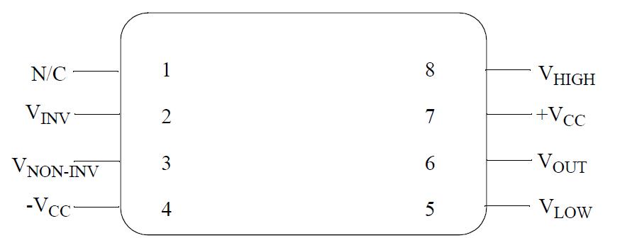
Features: · Output clamping (Vhigh and Vlow)
· 1ns recovery from clamping/overdrive
· 0.05% settling in 12ns
· Characterized and guaranteed at Av = +32
· Low power, 180mWApplication· Residue amplifier in high-accuracy, subranging A/D systems
· High-speed communications
· Output clamping applications
· Pulse amplitude modulation systemsPinout Specifications
Supply Voltage (Vs).......................................+7V dc
Output Current (Iout)......................................70mA
Junction Temperature (Tj).............................+175 C
Storage Temperature......................-65 C to +150 C
Lead Temperature (soldering, 10 seconds)..+300 C
Power Dissipation (Pd)
(Note 2).............................................................TBD
Common Mode Input Voltage (Vcm).....................Vs
Thermal Resistance
ThetaJA (Junction to Ambient)
CERAMIC DIP (Still Air) ......................................TBD
(500LFPM) ........................................................TBD
SOIC (Still Air) ...................................................TBD
(500LFPM) ........................................................TBD
ThetaJC (Juntion to Case)
CERAMIC DIP ....................................................TBD
SOIC .................................................................TBD
Package Weight
(Typical)
CERAMIC DIP ...................................................TBD
SOIC ................................................................TBD
ESD Tolerance
(Note 3)
ESD Rating................................................ <1000V
Note 1: Absolute Maximum Ratings are limits beyond which damage to the device may occur. Operating Ratings are conditions for which the device is functional, but do not guarantee specific performance limits. For guaranteed specifications and test conditions see the Electrical Characteristics. The guaranteed specifications apply only for the test conditions listed. Some performance characteristics may degrade when the device is not operated under the listed test conditions.
Note 2: The maximum power dissipation must be derated at elevated temperatures and is dictated by Tjmax (maximum junction temperature), ThetaJA (package junction to ambient thermal resistance), and TA (ambient temperature). The maximum allowable power dissipation at any temperature is Pdmax = (Tjmax - TA)/ThetaJA or the number given in the Absolute Maximum Ratings, whichever is lower.
Note 3: Human body model, 100pF discharged through 1.5K Ohms.
DescriptionThe CLC501 is a high-speed current-feedback op amp with the unique feature of output voltage clamping. This feature allows both the maximum positive (Vhigh) and negative (Vlow) output voltage levels to be established. This is useful in a number of applications in which "downstream" circuitry must be protected from overdriving input signals. Not only can this prevent damage to downstream circuitry, but can also reduce time delays since saturation is avoided. The CLC501's very fast 1ns overload/clamping recovery time is useful in applications in which information-containing signals follow overdriving signals.
Engineers designing high-resolution, subranging A/D systems have long sought an amplifier capable of meeting the demanding requirements of the residue amplifier function. Amplifiers providing the residue function must not only settle quickly, but recover from overdrive quickly, protect the second stage A/D, and provide high fidelity at relatively high gain settings. The CLC501, which excels in these areas, is the ideal design solution in this onerous application. To further support this application, the CLC501 is both characterized and tested at a gain setting of +32, the most common gain setting for residue amplifier applications.
The CLC501's other features provide a quick, high-performance design solution. Since the CLC501's current feedback design requires no external compensation, designers need not spend their time designing compensation networks. The small 8-pin package and low, 180mW power consumption make the CLC501 ideal in numerous applications having small power and size budgets.

 MNCLC501A-X Data Sheet


