Features: · 1.2GHz small-signal bandwidth (Av = +2)
· 2500V/us slew rate
· 0.03%, 0.02 Dg
· 6ns settling time to 0.2%
· 3rd order intercept, 30dBm @ 70MHz
· Dual +5V or single 10V supply
· High output current: 90mA
· 2.5dB noise figureApplication· High performance RGB video
· RF/IF amplifier
· Instrumentation
· Medical electronics
· Active filters
· High-speed A/D driver
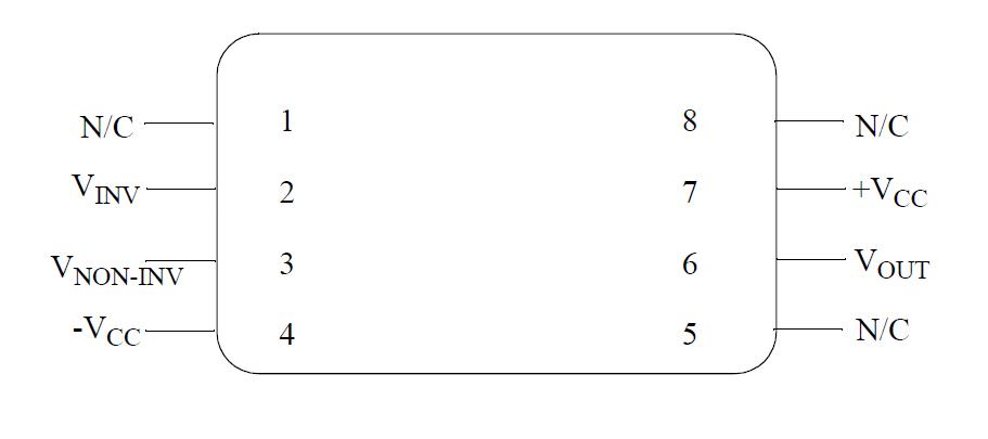
· High-speed D/A bufferPinout Specifications
Supply Voltage (Vcc)......................................+6V dc
Output Current (Iout)...................................+96mA
Common Mode Input Voltage.............................Vcc
Differential Input Voltage..................................+4V
Maximum Power Dissipation (Pd)
(Note 2)..........................................................1.2W
Junction Temperature (Tj)...........................+175 C
Storage Temperature Range..........-65 C to +150C
Lead Temperature (soldering, 10 seconds).+300 C
Thermal Resistance
Junction -to-ambient (ThetaJA)
Ceramic DIP (Still Air) .......................................TBD
(500 LFPM) ......................................................TBD
Junction -to-case (ThetaJC)
Ceramic DIP .....................................................TBD
Package Weight
(Typical)
Ceramic DIP .....................................................TBD
Note 1: Absolute Maximum Ratings are limits beyond which damage to the device may occur. Operating Ratings are conditions for which the device is functional, but do not guarantee specific performance limits. For guaranteed specifications and test conditions see the Electrical Characteristics. The guaranteed specifications apply only for the test conditions listed. Some performance characteristics may degrade when the device is not operated under the listed test conditions.
Note 2: The maximum power dissipation must be derated at elevated temperatures and is dictated by Tjmax (maximum junction temperature), ThetaJA (package junction to ambient thermal resistance), and TA (ambient temperature). The maximum allowable power dissipation at any temperature is Pdmax = (Tjmax - TA) / ThetaJA or the number given in the Absolute Maximum Ratings, whichever is lower.
Note 3: Human body model, 100 pF discharged through 1.5K Ohms.
DescriptionThe Comlinear CLC449 is an ultra-high-speed monolithic op amp, with a typical -3dB bandwidth of 1.2GHz at a gain of +2. This wideband op amp supports rise and fall times less than 1ns, settling time of 6ns (to 0.2%) and slew rate of 2500V/us. The CLC449 achieves 2nd harmonic distortion of -68dBc at 5MHz at a low supply current of only 12mA. These performance advantages have been achieved through improvements in Comlinear's proven current feedback topology combined with a high-speed complementary bipolar process. The DC to 1.2GHz bandwidth of the CLC449 is suitable for many IF and RF applications as a versatile op amp building block for replacement of AC coupled discrete designs. Operational amplifier functions such as active filters, gain blocks, differentiation, addition, subtraction and other signal conditioning functions take full advantage of the CLC449's unity-gain stable closed-loop performance.
The CLC449 performance provides greater headroom for lower frequency applications such as component video, high-resolution workstation graphics, and LCD displays. The amplifier's 0.1dB gain flatness to beyond 200MHz, plus 0.8ns 2V rise and fall times are ideal for improved time domain performance. In addition, the 0.03%/0.02 differential gain/phase performance allows system flexibility for handling standard NTSC and PAL signals. In applications using high-speed flash A/D and D/A converters, the CLC449 provides the necessary wide bandwidth (1.2GHz), settling (6ns to 0.2%) and low distortion into 50 Ohms loads to improve SFDR.

 MNCLC449A-X Data Sheet


