MNCLC432A-X

Features: · Wide bandwidth: 92Mhz (Av = +1) 62MHz (Av = +2)·Fast slew rate: 2000V/us·Fast disable: 1us to high-Z output·High channel isolation: 70dB at 10MHz·Single or dual supplies: +5V to +16.5VApplication·Video signal multiplexing·Twisted-pair differential driver·CCD buffer & level shifting...

product image

MNCLC432A-X Picture
SeekIC No. : 004424749 Detail

MNCLC432A-X: Features: · Wide bandwidth: 92Mhz (Av = +1) 62MHz (Av = +2)·Fast slew rate: 2000V/us·Fast disable: 1us to high-Z output·High channel isolation: 70dB at 10MHz·Single or dual supplies: +5V to +16.5VAp...

floor Price/Ceiling Price

Part Number:
MNCLC432A-X
Supply Ability:
5000

Price Break

  • Qty
  • 1~5000
  • Unit Price
  • Negotiable
  • Processing time
  • 15 Days
Total Cost: $ 0.00

SeekIC Buyer Protection PLUS - newly updated for 2013!

  • Escrow Protection.
  • Guaranteed refunds.
  • Secure payments.
  • Learn more >>

Month Sales

268 Transactions

Rating

evaluate  (4.8 stars)

Upload time: 2024/11/26

Payment Methods

All payment methods are secure and covered by SeekIC Buyer Protection PLUS.

Notice: When you place an order, your payment is made to SeekIC and not to your seller. SeekIC only pays the seller after confirming you have received your order. We will also never share your payment details with your seller.
Product Details

Description


Features:

· Wide bandwidth: 92Mhz (Av = +1) 62MHz (Av = +2)
· Fast slew rate: 2000V/us
· Fast disable: 1us to high-Z output
· High channel isolation: 70dB at 10MHz
· Single or dual supplies: +5V to +16.5V


Application

· Video signal multiplexing
· Twisted-pair differential driver
· CCD buffer & level shifting
· Discrete gain-select amplifier
· Transimpedance amplifier


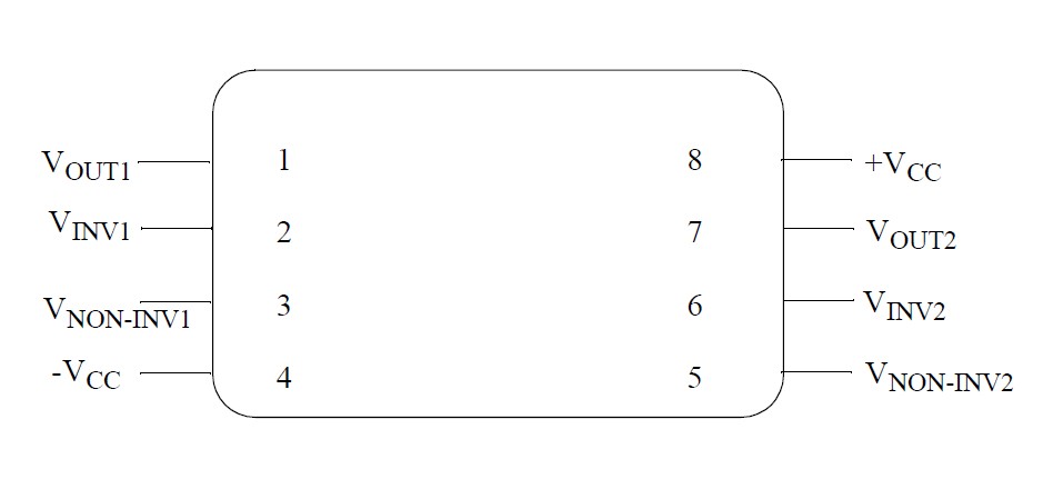
Pinout

  Connection Diagram


Specifications

Supply Voltage (Vs).........................................+16.5 V dc
Output Current (Iout)............................................100mA
Common Mode Input Voltage (Vcm)...........................+Vs
Differential Input Voltage(Vid)................................+10 V
Maximum Power Dissipation (Pd)
(Note 2)..................................................................1.02W
Lead Temperature
(Soldering, 10 seconds)....................................... +300 C
Junction Temperature (Tj).....................................+175 C
Storage Temperature Range...................-65 C to +150 C
Thermal Resistance
Junction -to-ambient (ThetaJA)
Ceramic DIP (Still Air) .........................................128 C/W
(500 LFPM) ...........................................................67 C/W
Junction -to-case (ThetaJC)
Ceramic DIP .........................................................23 C/W
Package Weight
(Typical)
Ceramic DIP ...............................................................TBD
ESD Tolerance
(Note 3)
ESD Ratings ..........................................................2000 V
Note 1: Absolute Maximum Ratings are limits beyond which damage to the device may occur. Operating Ratings are conditions for which the device is functional, but do not guarantee specific performance limits. For guaranteed specifications and test conditions see the Electrical Characteristics. The guaranteed specifications apply only for the test conditions listed. Some performance characteristics may degrade when the device is not operated under the listed test conditions.
Note 2: The maximum package power dissipation must be derated at elevated temperatures and is dictated by Tjmax (maximum junction temperature), ThetaJA (package junction to ambient thermal resistance), and TA (ambient temperature). The maximum allowable package power dissipation at any temperature is Pdmax = (Tjmax -TA) / ThetaJA or the number given in the Absolute Maximum Ratings, whichever is lower.
Note 3: Human body model, 100 pF discharged through 1.5K Ohms.


Description

The CLC432 is a current-feedback amplifier that provides a wide bandwidth and high slew rate for applications where board density and power are key considerations. This amplifier provides a dc-coupled small signal bandwidth exceeding 92MHz while consuming only 7mA per channel. Operating from +15V supplies, the CLC432's enhanced slew rate circuitry delivers large-signal bandwidths with output voltage swings up to 28Vpp. A wide range of bandwidth-insensitive gains are made possible by virtue of the CLC432's current-feedback topology.

The large common-mode input range and fast settling time (70ns to 0.05%) makes this amplifier well suited for CCD & data telecommunication applications. Many high performance video applications requiring signal gain and/or switching will be satisfied with the CLC432 due to it's very low differential gain and phase errors (less than 0.1% and 0.1 degrees; Av = +2V/V at 4.43MHz into 150Ohms load).

Quick 8ns rise and fall times on 10V pulses allow the CLC432 to drive either twisted pair or coaxial transmission lines over long distances.

The CLC432's combination of low input voltage noise, wide common-mode input voltage range and large output voltage swings makes it especially well suited for wide dynamic range signal processing applications.


Customers Who Bought This Item Also Bought

Margin,quality,low-cost products with low minimum orders. Secure your online payments with SeekIC Buyer Protection.
Cable Assemblies
Transformers
Industrial Controls, Meters
Semiconductor Modules
Hardware, Fasteners, Accessories
View more