MNCLC412A-X

Features: ·Wide bandwidth: 330MHz (Av=+1V/V) 250MHz (Av=+2V/V)·0.1dB gain flatness to 30MHz·- Low power: 5mA/channel·Very low diff. gain, phase: 0.02%, 0.02degrees·-76dB channel-to-channel crosstalk (10MHz)·Fast slew rate: 1300V/ms· Unity-gain stableApplication·HDTV, NTSC & PAL video systems·V...

product image

MNCLC412A-X Picture
SeekIC No. : 004424745 Detail

MNCLC412A-X: Features: ·Wide bandwidth: 330MHz (Av=+1V/V) 250MHz (Av=+2V/V)·0.1dB gain flatness to 30MHz·- Low power: 5mA/channel·Very low diff. gain, phase: 0.02%, 0.02degrees·-76dB channel-to-channel crosstalk...

floor Price/Ceiling Price

Part Number:
MNCLC412A-X
Supply Ability:
5000

Price Break

  • Qty
  • 1~5000
  • Unit Price
  • Negotiable
  • Processing time
  • 15 Days
Total Cost: $ 0.00

SeekIC Buyer Protection PLUS - newly updated for 2013!

  • Escrow Protection.
  • Guaranteed refunds.
  • Secure payments.
  • Learn more >>

Month Sales

268 Transactions

Rating

evaluate  (4.8 stars)

Upload time: 2024/11/26

Payment Methods

All payment methods are secure and covered by SeekIC Buyer Protection PLUS.

Notice: When you place an order, your payment is made to SeekIC and not to your seller. SeekIC only pays the seller after confirming you have received your order. We will also never share your payment details with your seller.
Product Details

Description


Features:

· Wide bandwidth: 330MHz (Av=+1V/V) 250MHz (Av=+2V/V)
· 0.1dB gain flatness to 30MHz
·- Low power: 5mA/channel
· Very low diff. gain, phase: 0.02%, 0.02degrees
· -76dB channel-to-channel crosstalk (10MHz)
· Fast slew rate: 1300V/ms
· Unity-gain stable


Application

· HDTV, NTSC & PAL video systems
· Video switching and distribution
·IQ amplifiers
· Wideband active filters
· Cable drivers
· DC coupled single-to-differential conversions


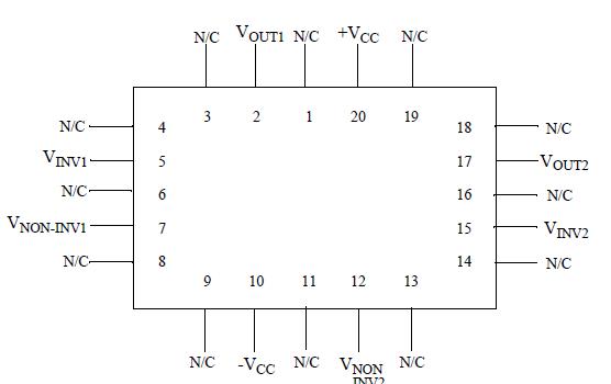
Pinout

  Connection Diagram


Specifications

Supply voltage(Vcc) ..........................................+7 V dc
Output current (Iout)...........................................96mA
Common mode input voltage (Vcm).......................+Vcc
Power dissipation (Pd)
(Note 2)............................................................201mW
Lead temperature (soldering, 10 seconds)........+300C
Junction temperature (Tj)...................................+175C
Storage temperature range..................-65C to +150C
Thermal Resistance
Junction-to-ambient (ThetaJA)
Ceramic DIP (Still Air) ............................................TBD
(500 LFPM) ............................................................TBD
LCC (Still Air) .........................................................TBD
(500 LFPM) ............................................................TBD
Junction-to-case (ThetaJC)
Ceramic DIP ..........................................................TBD
LCC .......................................................................TBD
Package Weight
(typical)
Ceramic DIP ..........................................................TBD
LCC .......................................................................TBD
ESD Tolerance
(Note 3).............................................................1000V
Note 1: Absolute Maximum Ratings are limits beyond which damage to the device may occur. Operating Ratings are conditions for which the device is functional, but do not guarantee specific performance limits. For guaranteed specifications and test conditions see the Electrical Characteristics. The guaranteed specifications apply only for the test conditions listed. Some performance characteristics may degrade when the device is not operated under the listed test conditions.
Note 2: The maximum power dissipation must be derated at elevated temperatures and is dictated by Tjmax (maximum junction temperature), ThetaJA (package junction to ambient thermal resistance), and TA (ambient temperature). The maximum allowable power dissipation at any temperature is Pdmax = (Tjmax - TA) /ThetaJA or the number given in the Absolute Maximum Ratings, whichever is lower.
Note 3: Human body model, 100pF discharged through 1.5k Ohms.


Description

The Comlinear CLC412 combines a high-speed complementary bipolar process with Comlinear's current-feedback topology to produce a very high-speed dual op amp. The CLC412 provides a 250MHz small-signal bandwidth at a gain of +2V/V and a 1300V/us slew rate while consuming only 50mW per amplifier from +5V supplies.

The CLC412 offers exceptional video performance with its 0.02% and 0.02 degrees differential gain and phase errors for NTSC and PAL video signals while driving one back terminated 75ohms load. The CLC412 also offers a flat gain response of 0.1dB to 30MHz and very low channel-to-channel crosstalk of -76dB at 10MHz. Additionally, each amplifier can deliver a 70mA continuous output current. This level of performance makes the CLC412 an ideal dual op amp for high-density broadcast-quality video systems.

The CLC412's two very well-matched amplifiers support a number of applications such as differential line drivers and receivers. In addition, the CLC412 is well suited for Sallen Key active filters in applications such as anti-aliasing filters for high-speed A/D converters. Its low power requirement, low noise and low distortion also allow the CLC412  to serve portable RF applications such as IQ-channels.


Customers Who Bought This Item Also Bought

Margin,quality,low-cost products with low minimum orders. Secure your online payments with SeekIC Buyer Protection.
Motors, Solenoids, Driver Boards/Modules
Circuit Protection
Cables, Wires
Memory Cards, Modules
View more