MN85560

Features: • Incorporates the image input filters used for front-end processing.• Supports PAL size images with just two external 16M synchronous DRAMs (SDRAM).• The back-end code output buffer is allocated in SDRAM and can be controlled from microcode.• Provides image quali...

product image

MN85560 Picture
SeekIC No. : 004424707 Detail

MN85560: Features: • Incorporates the image input filters used for front-end processing.• Supports PAL size images with just two external 16M synchronous DRAMs (SDRAM).• The back-end code o...

floor Price/Ceiling Price

Part Number:
MN85560
Supply Ability:
5000

Price Break

  • Qty
  • 1~5000
  • Unit Price
  • Negotiable
  • Processing time
  • 15 Days
Total Cost: $ 0.00

SeekIC Buyer Protection PLUS - newly updated for 2013!

  • Escrow Protection.
  • Guaranteed refunds.
  • Secure payments.
  • Learn more >>

Month Sales

268 Transactions

Rating

evaluate  (4.8 stars)

Upload time: 2024/11/26

Payment Methods

All payment methods are secure and covered by SeekIC Buyer Protection PLUS.

Notice: When you place an order, your payment is made to SeekIC and not to your seller. SeekIC only pays the seller after confirming you have received your order. We will also never share your payment details with your seller.
Product Details

Description


Features:

• Incorporates the image input filters used for front-end processing.
• Supports PAL size images with just two external 16M synchronous DRAMs (SDRAM).
• The back-end code output buffer is allocated in SDRAM and can be controlled from microcode.
• Provides image quality improvement functions:
• Multiple-mode high-performance motion vector detection
• Original rate control techniques implemented in microcode
• Intra-slice functions for low delay modes and PES output to reduce the system encoding load
• Clock input
• Three clocks: system clock SCLK (27 MHz), video input clock VCLK, and code output clock RCLK.
• An internal PLL circuit is used to generate an 81 MHz clock from SCLK (27 MHz). This clock is used for internal circuits and the synchronous DRAM.
• Supply voltages: 3.3 V (I/O supply voltage and internal PLL circuit supply voltage)
                             
1.8 V (internal circuit supply voltage)


Application

• DVD recorders, multimedia personal computers, MPEG2 cameras etc.


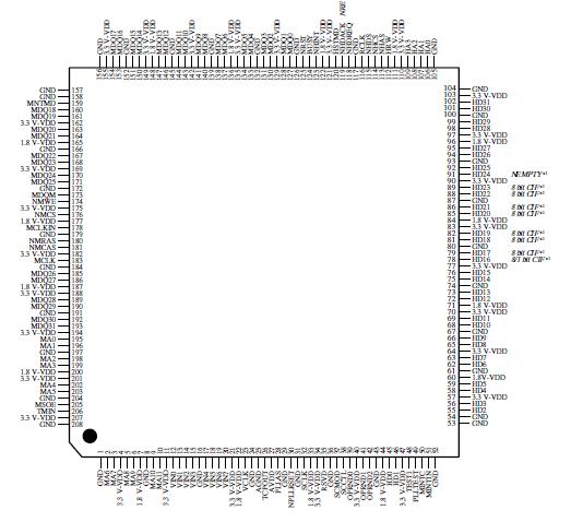
Pinout

  Connection Diagram


Specifications

Parameter

Symbol.

Conditions

Unit

Supply voltage 1

VDD

− 0.3 to +4.6

V

Supply voltage 2

VDDI

− 0.3 to +3.6

V

Supply voltage 3

AVDD

− 0.3 to +4.6

V

Input voltage

VI

− 0.3 to VDD + 0.3 (Upper limit: 4.6)

V

Output voltage

VO

− 0.3 to VDD + 0.3 (Upper limit: 4.6)

V

Average output current

IO

±24

mA

Power dissipation

PD

3.3 (layer 4)

W

Operating temperature

Topr

0 to +70

°C

Storage temperature

Tstg

−40 to +125

°C

Note) *1: MCLK and MCLKIN should be connected externally with a delay of 1 ns or less.
         *2: The bold notation in the HD pin I/O column indicates the I/O state immediately following a chip reset.
         *3: Items in italic indicate values immediately after a chip reset when MSOE is high.
         *4: The MD[31:0] values (all high) immediately following a chip reset are due to these lines being pulled up internally in the IC. Therefore, no problems will occur if the SDRAM is driving MD[31:0].


Description

The MN85560 is an MPEG2 video encoder that outputs encoded data that conform to the ISO/IEC 1318-2 (MPEG2 video) Main Profile@Main Level and ISO/IEC 1172-2 (MPEG1 video) standards.


Customers Who Bought This Item Also Bought

Margin,quality,low-cost products with low minimum orders. Secure your online payments with SeekIC Buyer Protection.
Audio Products
Cables, Wires - Management
Tapes, Adhesives
803
Connectors, Interconnects
Industrial Controls, Meters
Computers, Office - Components, Accessories
View more