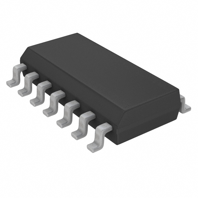
Features: TTL input characteristic compatible
Typical propagation delay: 18 ns
Low input current: 1 A maximum
Low quiescent current: 80 A maximum
Compatible with bus-oriented systems
Output drive capability: 15 LS-TTL loads
SpecificationsSupply Voltage (VCC ) -0.5 to,7.0V
DC Input Voltage (VIN ) -1.5 to VCC,1.5V
DC Output Voltage (VOUT ) -0.5 to VCC , 0.5V
Clamp Diode Current (IIK, IOK) ± 20 mA
DC Output Current, per pin (IOUT) ±35 mA
DC VCC or GND Current, per pin (ICC) ±70 mA
Storage Temperature Range (TSTG ) -65 to,150
Power Dissipation (PD)
(Note 3) 600 mW
S. O. Package only 500 mW
Lead Temperature (TL)
(Soldering 10 seconds) 260
Description The MM74HCT573 octal D-type latches and MM74HCT574 octal D-type flip-flop advanced silicon-gate CMOS technology, which provides the inherent benefits of low power consumption and wide power supply range, but are LS-TTL input and output characteristic and pin-out compatible. The 3-STATE outputs are capable of driving 15 LS-TTL loads. All inputs of MM74HCT573 are protected from damage due to static discharge by internal diodes to VCC and ground.
When the MM74HCT573 Latch Enable input is HIGH, the Q outputs will follow the D inputs. When the Latch Enable goes LOW, data at the D inputs will be retained at the out-puts until Latch Enable returns HIGH again. When a high logic level is applied to the Output Control input, all outputs of MM74HCT573 go to a high impedance state, regardless of what signals are present at the other inputs and the state of the storage elements.
The MM74HCT574 are positive edge triggered flip-flops.Data at the D inputs,meeting the setup and hold time requirements,are transferred to the Q outputs on positive going transitions of the Clock (CK) input. When a high logic level is applied to the Output Control (OC) input, all outputs go to a high impedance state, regardless of what signals are present at the other inputs and the state of the storage elements.
The MM74HCT573 are intended to interface between TTL and NMOS components and standard CMOS devices. These parts are also plug in replacements for LS-TTL devices and can be used to reduce power consumption in existing designs.

 MM74HCT573 Data Sheet


