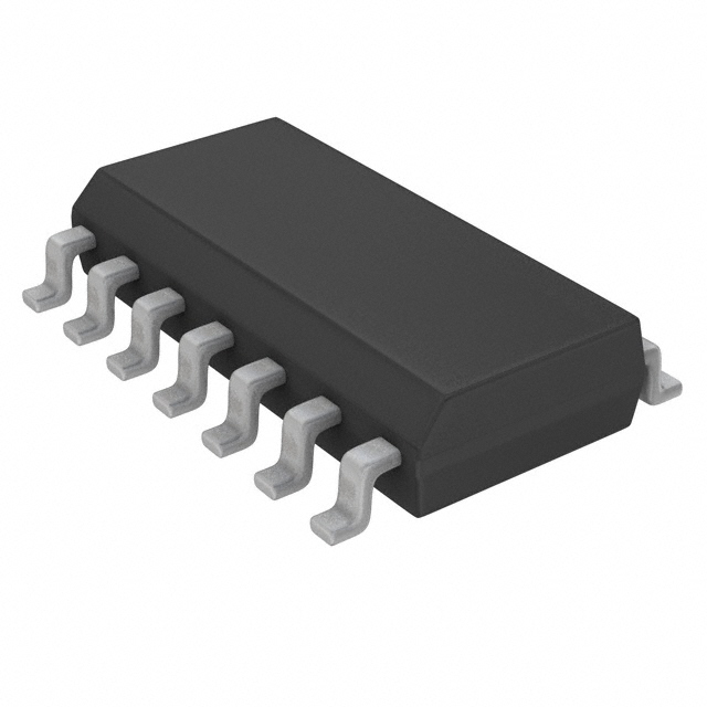
Features: Typical operating frequency: 50 MHz Typical propagation delay: 12 ns Wide operating supply voltage range: 2±6V Low input current: 1 mA maximum Low quiescent supply current: 80 mA maximum (74HC Series) Fanout of 10 LS-TTL loadsSpecifications Supply Voltage (VCC)DC Input Volt...
MM74HC75: Features: Typical operating frequency: 50 MHz Typical propagation delay: 12 ns Wide operating supply voltage range: 2±6V Low input current: 1 mA maximum Low quiescent supply current: 80 mA max...
SeekIC Buyer Protection PLUS - newly updated for 2013!
268 Transactions
All payment methods are secure and covered by SeekIC Buyer Protection PLUS.
Supply Voltage (VCC) DC Input Voltage (VIN) DC Output Voltage (VOUT) Clamp Diode Current (IIK, IOK) DC Output Current, per pin (IOUT) DC VCC or GND Current, per pin (ICC) Storage Temperature Range (TSTG) Power Dissipation (PD) (Note 3) S.O. Package only Lead Temp. (TL) (Soldering 10 seconds) |
-0.5 to +7.0V -1.5 to VCC+1.5V -0.5 to VCC+0.5V ±20 mA ±25 mA ±50 mA -65oC to a150oC 600 mW 500 mW 260oC |
This 4-bit latch MM74HC75 utilizes advanced silicon-gate CMOS technology to achieve the high noise immunity and low power consumption normally associated with standard CMOS integrated circuits. These devices can drive 10 LS-TTL loads. This latch is ideally suited for use as temporary storage for binary information processing, input/output, and indicator units. Information present at the data (D) input is transferred to the Q output when the enable (G) is high. The Q output of MM74HC75 will follow the data input as long as the enable remains high. When the enable goes low, the information that was present at the data input at the time the transition occurred is retained at the Q output until the enable is permitted to go high again.
The MM74HC75 is functionally as well as pinout compatible with the standard 54LS/74LS logic family. All inputs are protected from damage due to static discharge by internal diode clamps to VCC and ground.