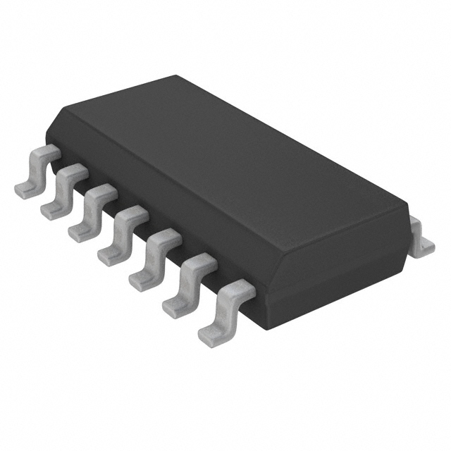
Features: Typical propagation delay: 14 ns
TRI-STATE outputs
Bidirectional communication
Wide power supply range: 2±6V
Low quiescent supply current: 160 mA maximum (74HC)
High output current: 6 mA (74HC)Specifications
|
Supply Voltage (VCC)
DC Input Voltage (VIN)
DC Output Voltage (VOUT)
Clamp Diode Current (IIK, IOK)
DC Output Current, per pin (IOUT)
DC VCC or GND Current, per pin (ICC)
Storage Temperature Range (TSTG)
Power Dissipation (PD)
(Note 3)
S.O. Package only
Lead Temp. (TL) (Soldering 10 seconds) |
-0.5 to +7.0V
-1.5 to VCC+1.5V
-0.5 to VCC+0.5V
±20 mA
±35 mA
±70 mA
-65oC to +150oC
600 mW
500 mW
260oC |
DescriptionThese transceivers MM74HC648 utilize advanced silicon-gate CMOS technology, and contain two sets of TRI-STATE. outputs, two sets of D-type flip-flops, and control circuitry designed for high speed multiplexed transmission of data. Six control inputs enable this MM74HC648 to be used as a latched transceiver, unlatched transceiver, or a combination of both. As a latched transceiver, data from one bus is stored for later retrieval by the other bus. Alternately real time bus data of MM74HC648 (unlatched) may be directly transferred from one bus to another.
Circuit operation of MM74HC648 is determined by the G, DIR, CAB, CBA, SAB, SBA control inputs. The enable input, G, controls whether any bus outputs are enabled. The direction control, DIR, determines which bus is enabled, and hence the direction data flows: The SAB, SBA inputs control whether the latched data (stored in D type flip flops), or the bus data (from other bus input pins) is transferred. Each set of flipflops has its own clock CAB, and CBA, for storing data. Data is latched on the rising edge of the clock.
Each output of MM74HC648 can drive up to 15 low power Schottky TTL loads. These devices are functionally and pin compatible to their LS-TTL counterparts. All inputs are protected from damage due to static discharge by diodes to VCC and ground.

 MM74HC648 Data Sheet


