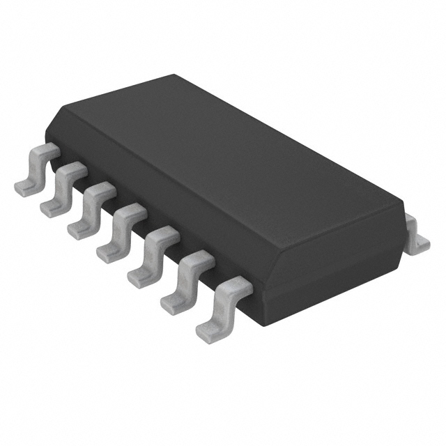
Supply Current
:
Maximum Power Dissipation
: 500 mW
Maximum Operating Temperature
: + 85 C
Minimum Operating Temperature
: - 40 C
Supply Voltage - Max
: 6 V
Supply Voltage - Min
: 2 V
Number of Channels
: 3 Channel
Packaging
: Tube
Propagation Delay Time
: 60 ns
Off Time (Max)
: 290 ns
Package / Case
: SOIC-16 Wide
On Resistance (Max)
: 230 Ohms
On Time (Max)
: 355 ns
DescriptionThe MM74HC4053WM contains 6 switches whose outputs are connected together in pairs, thus implementing a triple 2 channel multiplexer, or the equivalent of 3 singlepole-double throw configurations. Each of the A, B, or C select lines independently controls one pair of switches, selecting one of the two switches to be "on". The feature of MM74HC4053WM are as follows: (1)Wide analog input voltage range: ±6V; (2)Low "on" resistance: 50 typ. (VCCVEE = 4.5V), 30 typ. (VCCVEE = 9V); (3)Logic level translation to enable 5V logic with ±5V analog signals; (4)Low quiescent current: 80 mA maximum (74HC); (5)Matched Switch characteristic.
The absolute maximum ratings of the MM74HC4053WM are: (1)Supply Voltage (VCC): -0.5 to +7.5V; (2)Supply Voltage (VEE): +0.5 to -7.5V; (3)Control Input Voltage (VIN): -1.5 to VCC +1.5V; (4)Switch I/O Voltage (VIO): VEE -0.5 to VCC +0.5V; (5)Clamp Diode Current (IIK, IOK): ±20 mA; (6)Output Current, per pin (IOUT): ±25 mA; (7)VCC or GND Current, per pin (ICC): ±50 mA; (8)Storage Temperature Range (TSTG): -65°C to +150°C; (9)Power Dissipation (PD): 600 mW; (10)Lead Temperature (TL)(Soldering 10 seconds): 260°C.
The following is about the electrical characteristics of MM74HC4053WM: (1)minimum high level input voltage: 1.5V; (2)maximum low level input voltage: 0.5V; (3)Maximum "ON" Resistance: 160 at VINH = VIL, IS = 2.0 mA, VIS = VCC to VEE or 230 at VINH = VIL, IS = 2.0 mA, VIS = VCC to VEE; (4)Maximum "ON" Resistance matching: 25 at VCTL = VIL, VIS = VCC to GND; (5)maximum control input current: ±1.0A at VIN=VCC or GND, VCC = 2-6V; (6)maximum quiescent supply current: 8A at VIN=VCC or GND, IOUT=0A; (7)Maximum Switch "OFF" Leakage Current: ±60nA at VOS = VCCor VEE, VIS = VEEor VCC, VINH = VIH; (8)Maximum Switch "ON" Leakage Current: ±0.1A at VIS = VCC to VEE, VINH = VIL.
Parameters: | Technical/Catalog Information | MM74HC4053WM |
| Vendor | Fairchild Semiconductor |
| Category | Integrated Circuits (ICs) |
| Type | Multiplexer |
| Voltage Supply Source | Dual Supply |
| Voltage - Supply, Single/Dual (±) | ±2 V ~ 6 V |
| Circuit | 3 x 2:1 |
| On-State Resistance | 100 Ohm |
| Mounting Type | Surface Mount |
| Package / Case | 16-SOIC |
| Packaging | Tube |
| Current - Supply | 16A |
| Operating Temperature | -40°C ~ 85°C |
| Function | Multiplexer |
| Drawing Number | * |
| Lead Free Status | Lead Free |
| RoHS Status | RoHS Compliant |
| Other Names | MM74HC4053WM
MM74HC4053WM
|

 MM74HC4053WM Data Sheet


