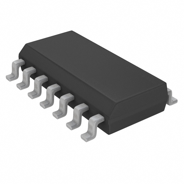
Features: Typical propagation delays - Select to outputs (4 delays): 18 ns - Select to output (5 delays): 28 ns - Enable to output: 20 ns Low power: 40 mW quiescent supply power Fanout of 10 LS-TTL devices Input current maximum 1 mA, typical 10 pASpecifications Supply Voltage (VCC)DC Input...
MM74HC139: Features: Typical propagation delays - Select to outputs (4 delays): 18 ns - Select to output (5 delays): 28 ns - Enable to output: 20 ns Low power: 40 mW quiescent supply power Fanout of 10 LS-TTL...
SeekIC Buyer Protection PLUS - newly updated for 2013!
268 Transactions
All payment methods are secure and covered by SeekIC Buyer Protection PLUS.
Supply Voltage (VCC) DC Input Voltage (VIN) DC Output Voltage (VOUT) Clamp Diode Current (IIK, IOK) DC Output Current, per pin (IOUT) DC VCC or GND Current, per pin (ICC) Storage Temperature Range (TSTG) Power Dissipation (PD) (Note 3) S.O. Package only Lead Temp. (TL) (Soldering 10 seconds) |
-0.5 to +7.0V -1.5 to VCC+1.5V -0.5 to VCC+0.5V ±20 mA ±25 mA ±50 mA -65oC to +150oC 600 mW 500 mW 260oC |
The MM74HC139 decoder utilizes advanced silicon-gate CMOS technology, and is well suited to memory address decoding or data routing applications. It possesses the high noise immunity and low power consumption usually associated with CMOS circuitry, yet has speeds comparable to low power Schottky TTL logic.
The MM74HC139 contain two independent one-of-four decoders each with a single active low enable input (G1, or G2). Data on the select inputs (A1, and B1 or A2, and B2) cause one of the four normally high outputs to go LOW. The decoder's outputs can drive 10 low power Schottky TTL equivalent loads, and are functionally as well as pin equivalent to the 74LS139. All inputs of MM74HC139 are protected from damage due to static discharge by diodes to VCC and ground.