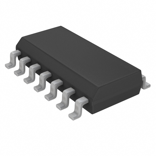
Features: ` Typical propagation delay: 13 ns
` Wide operating voltage range: 26V
` Low input current: 1 mA maximum
` Low quiescent current: 80 mA maximum (74HC)
`Fanout of 15 LS-TTL loads
SpecificationsSupply Voltage (VCC) -0.5 to +7.0V
DC Input Voltage (VIN) -1.5 to VCC +1.5V
DC Output Voltage (VOUT) -0.5 to VCC +0.5V
Clamp Diode Current (IIK, IOK) ±20 mA
DC Output Current, per pin (IOUT) ±35 mA
DC VCC or GND Current, per pin
(ICC) ±70 mA
Storage Temperature Range (TSTG)-65to +150
Power Dissipation (PD)
(Note 3) 600 mW
S.O. Package only 500 mW
Lead Temperature (TL)
(Soldering 10 seconds)260
Min Max Units
Supply Voltage (VCC)26 V
DC Input or Output Voltage 0 VCC V
(VIN, VOUT)
Operating Temperature Range (TA) -40 +85
Input Rise or Fall Times (tr, tf)
VCC = 2.0V1000ns
VCC = 4.5V 500ns
VCC = 6.0V400ns
Note 1: Absolute Maximum Ratings are those values beyond which damage to the device may occur.
Note 2: Unless otherwise specified all voltages are referenced to ground.
Note 3: Power Dissipation temperature derating - plastic "N" package: - 12 mW/from 65 to 85.
DescriptionThe MM74HC125 and MM74HC126 are general purpose 3-STATE high speed non-inverting buffers utilizing advanced silicon-gate CMOS technology. They have high drive current outputs which enable high speed operation even when driving large bus capacitances. These circuits of MM74HC125 possess the low power dissipation of CMOS circuitry, yet have speeds comparable to low power Schottky TTL circuits. Both circuits are capable of driving up to 15 low power Schottky inputs.
The MM74HC125 require the 3-STATE control input C to be taken high to put the output into the high impedance condition, whereas the MM74HC126 require the control input to be low to put the output into high impedance.
All inputs of MM74HC125 are protected from damage due to static discharge by diodes to VCC and ground.

 MM74HC125 Data Sheet


