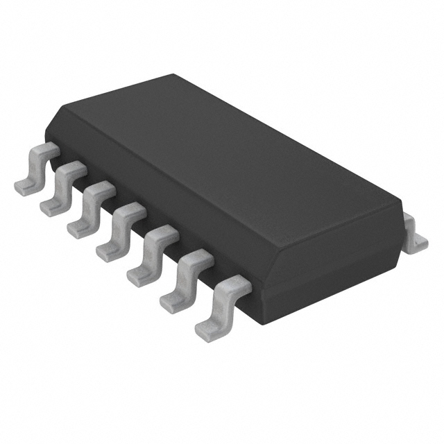
Features: Medium speed operation High noise immunity Low power Tenth power TTL compatible Wide supply voltage range Synchronous parallel load Parallel inputs and outputs from each flip-flop Negative edge triggered clocking The MM54C95/MM74C95 follows the MM54L95/MM74L95 PinoutApplication Data ter...
MM74C95: Features: Medium speed operation High noise immunity Low power Tenth power TTL compatible Wide supply voltage range Synchronous parallel load Parallel inputs and outputs from each flip-flop Negativ...
SeekIC Buyer Protection PLUS - newly updated for 2013!
268 Transactions
All payment methods are secure and covered by SeekIC Buyer Protection PLUS.
Voltage at Any Pin Operating Temperature Range MM54C95 MM74C95 Storage Temperature Range Power Dissipation Dual-In-Line Small Outline Operating VCC Range Absolute Maximum VCC Lead Temperature (Soldering, 10 seconds) |
- 0.3V to VCC + 0.3V - 55 to +125 - 40 to +85 - 65 to +150 700 mW 500 mW 3.0V to 15V 18V 260 |
This 4-bit shift register MM74C95 is a monolithic complementary MOS (CMOS) integrated circuit composed of four D flip-flops. This register will perform right-shift or left-shift operations dependent upon the logical input level to the mode control. A number of these registers MM74C95 may be connected in series to form an N-bit right-shift or left-shift register.
When a logical "0'' level is applied to the mode control input, the output of each flip-flop MM74C95 is coupled to the D input of the succeeding flip flop. Right-shift operation is performed by clocking at the clock 1 input, and serial data entered at the serial input, clock 2 and parallel inputs A through D are inhibited. With a logical "1'' level applied to the mode control, outputs to succeeding stages are decoupled and parallel loading is possible, or with external interconnection, shiftleft operation of MM74C95 can be accomplished by connecting the output of each flip-flop to the parallel input of the previous flip-flop and serial data is entered at input D.