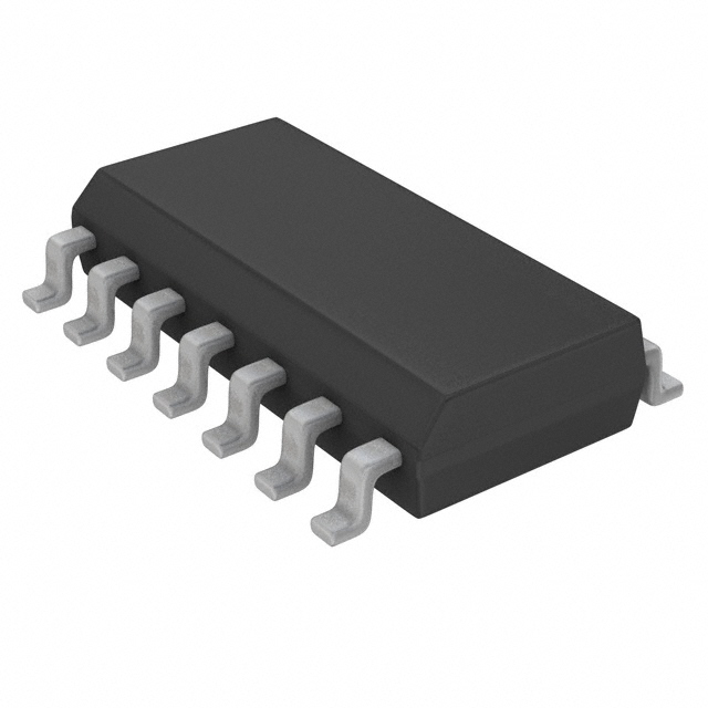
Features: · Medium speed operation 8.5 MHz (typ.) with 10V supply and 50 pF load· High noise immunity 0.45 VCC (typ.)· Low power 100 nW (typ.)· Tenth power TTL compatible Drive 2 LPTTL loads· Supply voltage range 3V to 15V· Synchronous parallel load· Parallel inputs and outputs from each flip-flop...
MM74C195: Features: · Medium speed operation 8.5 MHz (typ.) with 10V supply and 50 pF load· High noise immunity 0.45 VCC (typ.)· Low power 100 nW (typ.)· Tenth power TTL compatible Drive 2 LPTTL loads· Supply...
SeekIC Buyer Protection PLUS - newly updated for 2013!
268 Transactions
All payment methods are secure and covered by SeekIC Buyer Protection PLUS.
· Medium speed operation 8.5 MHz (typ.) with 10V supply and 50 pF load
· High noise immunity 0.45 VCC (typ.)
· Low power 100 nW (typ.)
· Tenth power TTL compatible Drive 2 LPTTL loads
· Supply voltage range 3V to 15V
· Synchronous parallel load
· Parallel inputs and outputs from each flip-flop
· Direct overriding clear
· J and K inputs to first stage
· Complementary outputs from last stage
· Positive-edge triggered clocking
Y Diode clamped inputs to protect against static charge
· Automotive
· Data terminals
· Instrumentation
· Medical electronics
· Alarm systems
· Remote metering
· Industrial electronics
· Computers
Voltage at any Pin |
-0.3V to VCC +0.3V |
Operating Temperature Range | |
MM54C195 |
-55 to +125 |
MM74C195 |
-40 to +85 |
Storage Temperature Range |
-65 to +150 |
Power Dissipation (PD) | |
Dual-In-Line |
700 mW |
Small Outline |
500 mW |
Operating VCC Range |
3V to 15V |
Absolute Maximum VCC |
18V |
Lead Temperature (Soldering, 10 sec.) |
260 |
The MM54C195/MM74C195 CMOS 4-bit registers feature parallel inputs, parallel outputs, J-K serial inputs, shift/load control input and a direct overriding clear. The following two modes of operation are possible: Parallel Load Shift in direction QA towards QD Parallel loading is accomplished by applying the four bits of data and taking the shift/load control of input low.
The data of MM74C195 is loaded into the associated flip-flops and appears at the outputs after the positive transition of the clock input. During parallel loading, serial data flow is inhibited.
Serial shifting of MM74C195 is accomplished synchronously when the shift/load control input is high. Serial data for this mode is entered at the J-K inputs. These inputs of MM74C195 allow the first stage to perform as a J-K, D, or T-type flip flop as shown in the truth table.