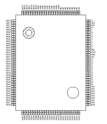
Features: • Logic voltage: VDD 2.7 to 5.5 V
• LCD drive voltage: VBI 6 to 16 V (positive voltage)
• 80 segment outputs,10 common outputs for ML9090-01 and 18 common outputs for ML9090- 02
• Built-in bit-mapped RAM (ML9090-01: 80 * 10 = 800 bits, ML9090-02: 80 * 18 = 1440 bits)
• 4-pin serial interface with CPU: CS, CP, DI/O, KREQ
• Built-in LCD drive bias resistors
• Built-in voltage doubler and tripler circuits
• Built-in 5 * 5 key scanner
• Port A output: 1 pin, output current: -15mA: (may be used for LED driving)
• Port B output: 8 pins, output current -2mA: each pin (general-purpose outputs), available for the ML9090-01 only
• Temperature range: 40 to +85°C
• Package: 128-pin plastic QFP (QFP128-P-1420-0.50-K)
- (Product name: ML9090-01GA)
- (Product name: ML9090-02GA)
Pinout Specifications
| Parameter |
Symbol |
Condition |
Rating |
Unit |
Applicable pins |
| Power Supply Voltage |
VDD |
Ta = 25°C |
0.3 to +7.0 |
V |
VDD |
| Bias Voltage |
VBI |
Ta = 25°C |
0.3 to +18.0 |
V |
VC1, VC2, VS1,
VS2, V2, V3A, V3B |
| Voltage Multiplier Reference |
VIN |
Ta = 25°C *1 |
0.3 to +9.0 |
V |
VIN |
| Voltage |
VIN |
Ta = 25°C *2 |
0.3 to +6.0 |
V |
VIN |
| Input Voltage |
VI |
Ta = 25°C |
0.3 to VDD+0.3 |
V |
CS, CP, DI/O,
OSC1, RESET, DT,
TEST, C0 to C4 |
| Output Current |
IO |
Ta = 25°C |
-20 |
mA |
PA0 |
| Output Current |
IO |
Ta = 25°C |
-3 |
mA |
PB0 to PB7 |
| Power Dissipation |
PD |
Ta = 85°C |
190 |
mW |
- |
| Storage Temperature Range |
Tstg |
- |
55 to +100 |
°C |
- |
*1: When Ta = 25°C and the voltage doubler is used, use voltage multiplier reference voltage VIN values within a range that does not exceed the power supply voltage VDD.
*2: When Ta = 25°C and the voltage tripler is used, use voltage multiplier reference voltage VIN values within a range that does not exceed the power supply voltage VDD.
DescriptionThe ML9090-01 and ML9090-02 are LCD drivers that contain internal RAM and a key scan function. They are best suited for car audio displays.
Since 1-bit data of the display RAM corresponds to the light-on or light-off of 1-dot of the LCD panel (a bit map system), a flexible display is possible.
A single chip ML9090-02 can implement a graphic display system of a maximum of 80 × 16 dots (80 ¥ 8 dots for the ML9090-01, 80 × 16 dots for the ML9090-02) and an arbitrator display system of 80 ×2 dots. Since containing voltage multipliers, the ML9090-01 and ML9090-02 require no power supply circuit to drive the LCD.
Since the internal 5 × 5 scan circuit of ML9090-02 has eliminated the needs of key scanning by the CPU, the ports of the CPU can be efficiently used.

 ML9090-02 Data Sheet


