Features: ` Precision buffered 5V reference (±0.5%)
` Current-input gain modulator reduces external components and improves noise immunity
` Programmable ramp compensation circuit
` 1A peak current totem-pole output drive
` Overvoltage comparator helps prevent output voltage "runaway"
` Wide common mode range in current sense comparators for better noise immunity
` Large oscillator amplitude for better noise immunity
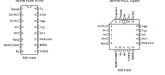
Pinout Specifications
Absolute maximum ratings are those values beyond which the device could be permanently damaged.Absolute maximum ratings are stress ratings only and functional device operation is not implied.
Supply Current (ICC) ............................................ 30mA
Output Current Source or Sink (OUT) DC................ 1.0A
Output Energy (capacitive load per cycle) ............... 5µJ
Gain Modulator ISINE Input (ISINE) .....................1.2mA
Error Amp Sink Current (EA OUT) ..........................10mA
Oscillator Charge Current .......................................2mA
Analog Inputs (ISENSE, EA, OVP) .........0.3V to 5.5V
Junction Temperature ........................................ 150°C
Storage Temperature Range ............ 65°C to 150°C
Lead Temperature (soldering 10 sec.) ............... 260°C
Thermal Resistance (JA)
20-Pin PLCC.................................................... 60°C/W
16-Pin PDIP .................................................... 65°C/W
DescriptionThe ML4812_1245284 is designed to optimally facilitate a peak current control boost type power factor correction system. Special care has been taken in the design of the ML4812_1245284 to increase system noise immunity. The circuit ML4812_1245284 includes a precision reference, gain modulator, error amplifier, over-voltage protection, ramp compensation, as well as a high current output. In addition, start-up is simplified by an under-voltage lockout circuit with 6V hysteresis.
In a typical application, the ML4812_1245284 functions as a current mode regulator. The current which is necessary to terminate the cycle is a product of the sinusoidal line voltage times the output of the error amplifier which is regulating the output DC voltage. Ramp compensation of ML4812_1245284 is programmable with an external resistor, to provide stable operation when the duty cycle exceeds 50%.

 ML4812_1245284 Data Sheet


