MK3711

Features: • MK3711D and MK3711B are drop-in replacements for the earlier MK3711S and MK3711A devices• MK3711D and MK3711B offer 24-36 MHz output frequency range (output frequency = 2x crystal frequency) and improved power supply noise rejection• Uses an inexpensive 12 to 18 MHz e...

product image

MK3711 Picture
SeekIC No. : 004421726 Detail

MK3711: Features: • MK3711D and MK3711B are drop-in replacements for the earlier MK3711S and MK3711A devices• MK3711D and MK3711B offer 24-36 MHz output frequency range (output frequency = 2x cr...

floor Price/Ceiling Price

Part Number:
MK3711
Supply Ability:
5000

Price Break

  • Qty
  • 1~5000
  • Unit Price
  • Negotiable
  • Processing time
  • 15 Days
Total Cost: $ 0.00

SeekIC Buyer Protection PLUS - newly updated for 2013!

  • Escrow Protection.
  • Guaranteed refunds.
  • Secure payments.
  • Learn more >>

Month Sales

268 Transactions

Rating

evaluate  (4.8 stars)

Upload time: 2024/11/21

Payment Methods

All payment methods are secure and covered by SeekIC Buyer Protection PLUS.

Notice: When you place an order, your payment is made to SeekIC and not to your seller. SeekIC only pays the seller after confirming you have received your order. We will also never share your payment details with your seller.
Product Details

Description


Features:

• MK3711D and MK3711B are drop-in replacements for the earlier MK3711S and MK3711A devices
• MK3711D and MK3711B offer 24-36 MHz output frequency range (output frequency = 2x crystal frequency) and improved power supply noise rejection
• Uses an inexpensive 12 to 18 MHz external crystal
• Ideal for ADSL applications using 17.664 MHz external pullable crystal to generate locked 35.328 MHz clock physical layer clock
• Ideal for set-top box applications using 13.5 MHz external pullable crystal to generate lock 27 MHz clock transport video clock
• On-chip VCXO with guaranteed pull range of ±115 ppm minimum (MK3711D)
• VCXO tuning voltage 0 to 3.3 V
• Packaged in 8 pin SOIC (150 mil wide)


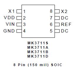
Pinout

  Connection Diagram


Specifications

Stresses above the ratings listed below can cause permanent damage to the MK3711. These ratings, which are standard values for ICS commercially rated parts, are stress ratings only. Functional operation of the device at these or any other conditions above those indicated in the operational sections of the specifications is not implied. Exposure to absolute maximum rating conditions for extended periods can affect product reliability. Electrical parameters are guaranteed only over the recommended operating temperature range.

Item
Rating
Supply Voltage, VDD 7 V
All Inputs and Outputs -0.5 V to VDD+0.5 V
Ambient Operating Temperature 0 to +70
Storage Temperature -65 to +150
Soldering Temperature 260


Description

The MK3711 series of devices include the original, MK3711A, and the new MK3711B and MK3711D. That and MK3711B are drop-in replacements for it and MK3711A devices. Compared to these earlier devices the MK3711D and MK3711B offer a wider operating frequency range and improved power supply noise rejection.

The MK3711 series combines the functions of a VCXO (Voltage Controlled Crystal Oscillator) and PLL (Phase Locked Loop) frequency doubler onto a single chip. Used in conjunction with an external pullable quartz crystal, this monolithic integrated circuit replaces more costly hybrid (canned) VCXO devices. The MK3711 is designed primarily for data and clock recovery applications within end products such as ADSL modems, set-top box receivers, and telecom systems.

The MK3711D exhibits a moderate VCXO gain of 120ppm/V typical, when used with a high quality external pullable quartz crystal. The MK3711B offers a higher VCXO gain of 150ppm/V, similar to the earlier MK3711A. The higher intrinsic VCXO gain of the MK3711C may help compensate for the reduced pullability of a low quality crystal used in some applications. However, higher VCXO gain may also increase clock output phase noise.

The frequency of the on-chip VCXO MK3711 is adjusted by an external control voltage input into pin VIN. Since VIN is a high impedance input, it can be driven directly from an PWM RC integrator circuit. Frequency output increases with VIN voltage input. The usable range of VIN is 0 to 3V.


Customers Who Bought This Item Also Bought

Margin,quality,low-cost products with low minimum orders. Secure your online payments with SeekIC Buyer Protection.
Integrated Circuits (ICs)
Potentiometers, Variable Resistors
Programmers, Development Systems
Undefined Category
Line Protection, Backups
View more