Features: • High sensitivity (104dBm)
• 300MHz to 440MHz frequency range
• Data-rate up to 2.0kbps (Manchester encoding)
• Low power consumption
2.9mA fully operational (315MHz)
0.15A in shutdown
290A in polled mode (10:1 duty-cycle)
• Shutdown input
• Automatic tuning, no manual adjustment
• Very low RF re-radiation at the antenna
• Highly integrated with extremely low external part countApplication• Automotive remote keyless entry (RKE)
• Long range RF identification
• Remote fan and light control
• Garage door and gate openersPinout
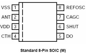
|

| Pin Number |
Pin Name |
Pin Function |
|
1 |
VSS |
Ground Return (input): ground return to the power supply. See "Applications Information" for bypass capacitor details. |
|
2 |
ANT |
Antenna (Input): See "Applications Information" for information on input impedance. For optimal performance the antenna impedance should be matched to the antenna pin impedance. |
|
3 |
VDD |
Power Supply (Input): Positive Supply input for the RF IC. Connect a low ESL, low ESR decoupling capacitor from this to VSS, with lead length kept as short as possible. |
|
4 |
CTH |
[Data Slicing] Threshold Capacitor (External Component): Capacitor extracts the DC average value from the demodulated waveform, which becomes the reference for the internal data slicing comparator. See "Applications Information" for selection. |
|
5 |
DO |
Digital Output (Output): CMOS level compatible data output signal. |
|
6 |
SHUT |
Shutdown (Input): Shutdown-mode logic-level control input. Pull low to enable the receiver. This input is pulled-up internally to VDD. |
|
7 |
CAGC |
AGC Capacitor (External Component): Integrating capacitor for on-chip AGC (automatic gain control). See "Applications Information" for capacitor selection. |
|
8 |
REFOSC |
Reference Oscillator (External Component or Input): Timing reference for on-chip tuning and alignment. | |
|
|
|
|
|
|
|
|
|
|
|
|
|
|
|
|
|
|
|
|
|
|
|
|
|
|
|
|
|
|
|
|
|
|
|
|
|
|
|
|
|
|
|
SpecificationsSupply Voltage (VDDRF, VDDBB).............................................+7V
Input/Output Voltage (VI/O)......................VSS0.3 to VDD+0.3
Max Input Power...........................................................+20dBm
Junction Temperature (TJ).............................................+150°C
Storage Temperature Range (TS)................65°C to +150°C
Lead Temperature (soldering, 10 sec.).........................+260°C
ESD Rating.......................................................................Note 3DescriptionThe MICRF010 is a single chip, ASK/OOK (ON-OFF Keyed) RF receiver IC recommended for new designs replacing the MICRF007. It provides the same function with sensitivity enhancement, typically 6dB better than the MICRF007. Just like all other members of the QwikRadio® family, the MICRF010 achieves low power operation, a very high level of integration, and it is particularly easy to use.
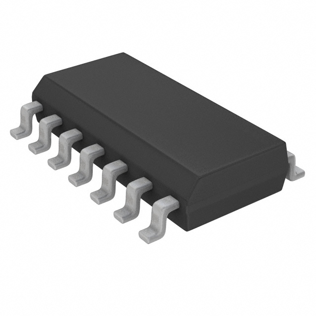
All post-detection data filtering is provided on the MICRF010, so no external baseband filters are required. In fact, the entire receiver circuit is made of very few external components and with the 8-pin SOIC package makes it ideal for small printed circuit board area applications.
The MICRF010 works in fixed-mode (FIX) operation, which functions as a conventional super-heterodyne receiver. Fixed-mode provides better selectivity and sensitivity performance in comparison with sweep mode used in other Micrel receivers intended for lower cost applications.
Data sheets and support documentation of MICRF010 can be found on Micrel's web site at www.micrel.com.

 MICRF010 Data Sheet


