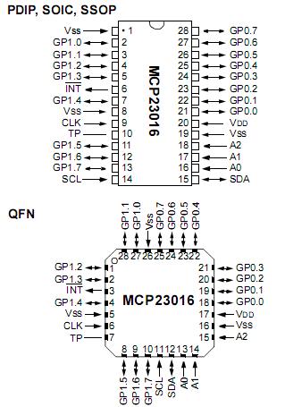
Features: `16-bit remote bidirectional I/O port
-16 I/O pins default to 16 inputs
`Fast I2CTM bus clock frequency (0 - 400kbits/s)
`Three hardware address pins allow use of up to eight devices
`High-current drive capability per I/O: ±25m
`Open-drain interrupt output on input change
`Interrupt port capture register
`Internal Power-On Reset (POR)
`Polarity inversion register to configure the polarity of the input port data
`Compatible with most microcontrollers
`Available temperature range:
-Industrial (I): -40 to +85
Pinout Specifications
| Device Description |
16-bit I/O Port Expander |
| Operating Voltage Range (V) |
2.0 to 5.5 |
| Operating Temp Range (°C) |
-40 to 85 |
| Interface |
I²C™ |
| Max. Bus Frequency (kBits/s) |
400 |
Absolute Maximum Ratings †
Ambient temperature under bias.............................. -55 to +125°C
Storage temperature .......................................... -65°C to +150°C
Voltage on any pin with respect to VSS ............ -0.3V to (VDD + 0.3V)
Voltage on VDD with respect to VSS ........................... -0.3V to +6.5V
Total power dissipation (Note 1) ............................................. 1.0 W
Maximum current out of VSS pin ............................................ 300 mA
Maximum current into VDD pin ............................................... 250 mA
Input clamp current, IIK (VI < 0, or VI > VDD) ...................... ± 20 mA
Output clamp current, IOK (VO < 0, or VO > VDD) ................ ± 20 mA
Maximum output current sunk by any I/O pin.......................... 25 mA
Maximum output current sourced by any I/O pin .................... 25 mA
Maximum current sunk by combined PORTS .......................... 200 mA
Maximum current sourced by combined PORTS ..................... 200 mA
Note 1: Power dissipation is calculated as follows:
Pdis = VDD x {IDD - IOH} + {(VDD-VOH) x IOH} + (VOl x IOL)
† NOTICE: Stresses above those listed under "Absolute Maximum Ratings" may cause permanent damage to the
device. This is a stress rating only and functional operation of the device at those or any other conditions above those
indicated in the operation listings of this specification is not implied. Exposure to maximum rating conditions for
extended periods may affect device reliability.
DescriptionThe MCP23016 device provides 16-bit, general purpose, parallel I/O expansion for I
2C?Compatible bus applications. MCP23016 includes high-current drive capability, low supply current and individual I/O configuration. I/O expanders provide a simple solution when additional I/Os are needed for ACPI, power switches, sensors, push buttons, LEDs and so on.

 MCP23016 Data Sheet


