Features: Single 3.3 V + 10%, 5% Power SupplyPlug and Pin Compatibility with 2MB and 4MBMultiple Clock Pins for Reduced LoadingAll Inputs and Outputs are LVTTL CompatibleByte Write CapabilityFast SRAM Access Times:9/10/12 nsDecoupling Capacitors for Each Fast Static RAMHigh Quality MultiLayer FR4...
MCM72F7: Features: Single 3.3 V + 10%, 5% Power SupplyPlug and Pin Compatibility with 2MB and 4MBMultiple Clock Pins for Reduced LoadingAll Inputs and Outputs are LVTTL CompatibleByte Write CapabilityFast S...
SeekIC Buyer Protection PLUS - newly updated for 2013!
268 Transactions
All payment methods are secure and covered by SeekIC Buyer Protection PLUS.
Rating | Symbol | Value | Unit |
Power Supply Voltage | VDD | 0.5 to + 4.6 | V |
Voltage Relative to VSS | Vin, Vout | 0.5 to VDD + 0.5 | V |
Output Current (per I/O) | Iout | ±20 | mA |
Power Dissipation MCM72F6 MCM72F7 |
PD | 4.6 9.2 |
W |
Ambient Temperature | TA | 0 to 70 | °C |
Die Temperature | TJ | 110 | °C |
Temperature Under Bias | Tbias | 10 to + 85 | °C |
Storage Temperature | Tstg | 55 to + 125 | °C |
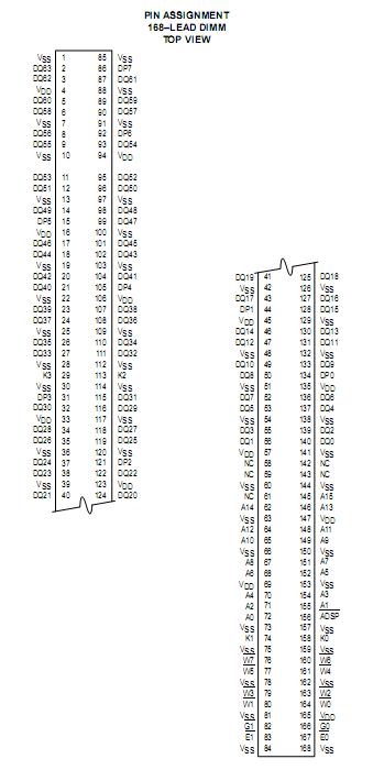
The MCM72F6 (512KB) is configured as 64K x 72 bits and the MCM72F7(1MB) is configured as 128K x 72 bits. Both are packaged in a 168pin dualinline memory module DIMM. Each module uses Motorola's 3.3 V 64K x 18 bitflowthrough BurstRAMs.
Address (A), data inputs (DQ, DP) of the MCM72F7, and all control signals except output enable(G) are clock (K) controlled through positiveedgetriggered noninverting reg-isters.
Write cycles of the MCM72F7 are internally selftimed and initiated by the rising edge of the clock (K) input. This feature provides increased timing flexibility for incoming signals. Synchronous byte write (W) allows writes to either individual bytes or to both bytes.