Features: • VGA resolution, active CMOS image sensor with square pixel unit cells• 7.8m pitch pixels with patented pinned photodiode architecture• Bayer-RGB color filter array with optional micro lenses• High sensitivity, quantum efficiency, and charge conversion efficiency...
MCM20014: Features: • VGA resolution, active CMOS image sensor with square pixel unit cells• 7.8m pitch pixels with patented pinned photodiode architecture• Bayer-RGB color filter array with...
SeekIC Buyer Protection PLUS - newly updated for 2013!
268 Transactions
All payment methods are secure and covered by SeekIC Buyer Protection PLUS.
Symbol |
Parameter |
Value |
Unit |
VDD |
DC Supply Voltage |
-0.5 to 3.8 |
V |
Vin |
DC Input Voltage |
0.5 to VDD + 0.5 |
V |
Vout |
DC Output Voltage |
-0.5 to VDD + 0.5 |
V |
I |
DC Current Drain per Pin, Any Single Input or Output |
±50 |
mA |
I |
DC Current Drain, VDD and VSS Pins |
±100 |
mA |
TSTG |
Storage Temperature Range |
-65 to +150 |
°C |
TL |
Lead Temperature (10 second soldering) |
300 |
°C |
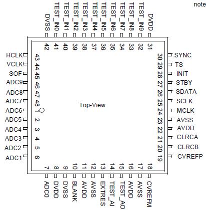
The MCM20014 is a fully integrated, high performance CMOS image sensor with features such as integrated timing control, and analog signal processing for digital imaging applications. The part provides designers a complete imaging solution with a monolithic image capture and processing engine thus making it a true "camera on a chip". System benefits enable design of smaller, portable, low cost and low power systems. Thereby making the product suitable for a variety of consumer applications including still/full motion imaging, security/surveillance, and automotive among others.
The imaging pixels are based on active CMOS pixels using pinned photodiodes that are realized using Motorola,s sub-micron ImageMOSTM technology. The frame rate is completely adjustable from 0 to 30 frames per second without adjusting the system clock from 10Mhz. Each pixel on the sensor is individually addressable allowing the user to control "Window of Interest" (WOI) panning and zooming, sub-sampling, resolution, exposure, gain, and other image processing features via a two pin I2C interface. Programmable digital signal processing blocks included in the data path are bad-pixel replacement and noise compensation for image enhancement. The sensor is run by supplying a single Master Clock. The sensor output is 8 or 10 digital bits depending on output mode selected.