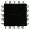
Features: The user must be reminded that part of the security must lie with the application code. An extreme example would be application code that dumps the contents of the internal memory. This would defeat the purpose of security. At the same time, the user may also wish to put a backdoor in th...
MC9S12XEP100: Features: The user must be reminded that part of the security must lie with the application code. An extreme example would be application code that dumps the contents of the internal memory. This wo...
SeekIC Buyer Protection PLUS - newly updated for 2013!
268 Transactions
All payment methods are secure and covered by SeekIC Buyer Protection PLUS.
US $1.61 - 2.56 / Piece
8-bit Microcontrollers (MCU) 8 Bit 128K FLASH 8K RAM
US $1.73 - 2.75 / Piece
8-bit Microcontrollers (MCU) 8 Bit 128K FLASH 8K RAM
US $1.74 - 2.77 / Piece
8-bit Microcontrollers (MCU) 8 Bit 128K FLASH 8K RAM
The user must be reminded that part of the security must lie with the application code. An extreme example would be application code that dumps the contents of the internal memory. This would defeat the purpose of security. At the same time, the user may also wish to put a backdoor in the application program. An example of this is the user downloads a security key through the SCI, which allows access to a programming routine that updates parameters stored in another section of the Flash memory.
The security features of the S12XE chip family (in secure mode) are:
• Protect the content of non-volatile memories (Flash, EEPROM)
• Execution of NVM commands is restricted
• Disable access to internal memory via background debug module (BDM)
• Disable access to internal Flash/EEPROM in expanded modes
• Disable debugging features for the CPU and XGATE
Num | Rating | Symbol | Min | Max | Unit |
1 | I/O, regulator and analog supply voltage | VDD35 | 0.3 | 6.0 | V |
2 | Digital logic supply voltage2 | VDD | 0.3 | 2.16 | V |
3 | PLL supply voltage2 | VDDPLL | 0.3 | 2.16 | V |
4 | NVM supply voltage2 | VDDF | 0.3 | 3.6 | V |
5 | Voltage difference VDDX to VDDA | VDDX | 6.0 | 0.3 | V |
6 | Voltage difference VSSX to VSSA | VSSX | 0.3 | 0.3 | V |
7 | Digital I/O input voltage | VIN | 0.3 | 6.0 | V |
8 | Analog reference | VRH, VRL | 0.3 | 6.0 | V |
9 | EXTAL, XTAL | VILV | 0.3 | 2.16 | V |
10 | TEST input | VTEST | 0.3 | 10.0 | V |
11 | Instantaneous maximum current Single pin limit for all digital I/O pins3 |
ID | 25 | +25 | mA |
12 | Instantaneous maximum current Single pin limit for EXTAL, XTAL4 |
IDL | 25 | +25 | mA |
13 | Instantaneous maximum current Single pin limit for TEST 5 |
IDT | 0.25 | 0 | mA |
14 | Storage temperature range | Tstg | 65 | 155 |
1 Beyond absolute maximum ratings device might be damaged.
2 The device contains an internal voltage regulator to generate the logic and PLL supply out of the I/O supply. The absolute maximum ratings apply when the device is powered from an external source.
3 All digital I/O pins are internally clamped to VSSX and VDDX, or VSSA and VDDA.
4 Those pins are internally clamped to VSSPLL and VDDPLL.
5 This pin is clamped low to VSSPLL, but not clamped high. This pin must be tied low in applications.
This specification MC9S12XEP100 describes the function of the security mechanism in the S12XE chip family (9SEC).
NOTE
No security feature is absolutely secure. However, Freescale's strategy is to make reading or copying the FLASH and/or EEPROM difficult for unauthorized users.