Features: • HCS12 Core
16-bit HCS12 CPU
i. Upward compatible with M68HC11 instruction set
ii. Interrupt stacking and programmer's model identical to M68HC11
iii.20-bit ALU
iv. Instruction queue
v. Enhanced indexed addressing
MEBI (Multiplexed External Bus Interface)
MMC (Module Mapping Control)
INT (Interrupt control)
BKP (Breakpoints)
BDM (Background Debug Mode)
• CRG (low current oscillator, PLL, reset, clocks, COP watchdog, real time interrupt, clock monitor)
• 8-bit and 4-bit ports with interrupt functionality
Digital filtering
Programmable rising or falling edge trigger
• Memory
128K, 256K Flash EEPROM
2K, 4K byte EEPROM
6K, 12K byte RAM
• Analog-to-Digital Converter
8, 16 channels, 10-bit resolution
External conversion trigger capability
• Two 1M bit per second, CAN 2.0 A, B software compatible modules
Five receive and three transmit buffers
Flexible identifier filter programmable as 2 x 32 bit, 4 x 16 bit or 8 x 8 bit
Four separate interrupt channels for Rx, Tx, error and wake-up
Low-pass filter wake-up function
Loop-back for self test operation
• Timer
16-bit main counter with 7-bit prescaler
8 programmable input capture or output compare channels
Two 8-bit or one 16-bit pulse accumulators
• 2, 6 PWM channels
Programmable period and duty cycle
8-bit 2, 6-channel or 16-bit 1, 3-channel
Separate control for each pulse width and duty cycle
Center-aligned or left-aligned outputs
Programmable clock select logic with a wide range of frequencies
Fast emergency shutdown input
• Serial interfaces
Two asynchronous Serial Communications Interfaces (SCI)
Synchronous Serial Peripheral Interface (SPI)
Inter-Integrated Circuit interface (IIC)
• Liquid Crystal Display driver with variable input voltage
Configurable for up to 32 frontplanes and 4 backplanes or general purpose input or output
5 modes of operation allow for different display sizes to meet application requirements
Unused frontplane and backplane pins can be used as general purpose I/O
• 16, 24 high current drivers suited for PWM motor control
Each PWM channel switchable between two drivers in an H-bridge configuration
Left, right and center aligned outputs
Support for sine and cosine drive
Dithering
Output slew rate control
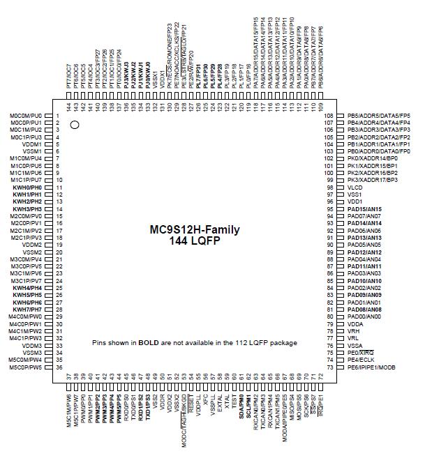
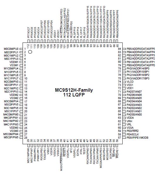
• 144-Pin or 112-Pin LQFP package
I/O lines with 5V input and drive capability
5V A/D converter inputs
Operation at 32MHz equivalent to 16MHz Bus Speed
Development support
Single-wire background debug™ mode (BDM)
On-chip hardware breakpointsPinout
 Specifications
| Rating |
Symbol |
Min |
Max |
Unit |
| I/O, Regulator and Analog Supply Voltage |
VDD5 |
0.3 |
6.0 |
V |
| Digital Logic Supply Voltage 2 |
VDD |
0.3 |
3.0 |
V |
| PLL Supply Voltage 2 |
VDDPLL |
0.3 |
3.0 |
V |
| Voltage difference VDDX1 to VDDX2 to VDDM and VDDA |
DVDDX |
0.3 |
0.3 |
V |
| Voltage difference VSSX to VSSR and VSSA |
DVSSX |
0.3 |
0.3 |
V |
| Digital I/O Input Voltage |
VIN |
0.3 |
6.0 |
V |
| Analog Reference |
VRH, VRL |
0.3 |
6.0 |
V |
| XFC, EXTAL, XTAL inputs |
VILV |
0.3 |
3.0 |
V |
| TEST input |
VTEST |
0.3 |
10.0 |
V |
| Instantaneous Maximum Current Single pin limit for all digital I/O pins except PU, PV and PW 3 |
ID |
25 |
+25 |
mA |
| Instantaneous Maximum Current Single pin limit for Port PU, PV and PW 4 |
ID |
55 |
+55 |
mA |
| Instantaneous Maximum Current Single pin limit for XFC, EXTAL, XTAL5 |
IDL |
25 |
+25 |
mA |
| Instantaneous Maximum Current Single pin limit for TEST 6 |
IDT |
0.25 |
0 |
mA |
| Storage Temperature Range |
Tstg |
65 |
155 |
°C |
NOTES:
1. Beyond absolute maximum ratings device might be damaged.
2. The device contains an internal voltage regulator to generate the logic and PLL supply out of the I/O supply. The absolute maximum ratings apply when the device is powered from an external source.
3. All digital I/O pins are internally clamped to VSSX1/2 and VDDX1/2, VSSM and VDDM or VSSA and VDDA.
4. Ports PU, PV, PW are internally clamped to VSSM and VDDM.DescriptionThe MC9S12H256 microcontroller unit (MCU) is a 16-bit device composed of standard on-chip peripherals including a 16-bit central processing unit (HCS12 CPU), 256K bytes of Flash EEPROM, 12K bytes of RAM, 4K bytes of EEPROM, two asynchronous serial communications interfaces (SCI), a serial peripheral interface (SPI), an IIC-bus interface (IIC), an 8-channel 16-bit timer (TIM), a 16-channel, 10-bit analog-to-digital converter (ATD), a six-channel pulse width modulator (PWM), and two CAN 2.0 A, B software compatible modules (MSCAN).
The MC9S12H128 microcontroller unit (MCU) is a 16-bit device composed of standard on-chip peripherals including a 16-bit central processing unit (HCS12 CPU), 128K bytes of Flash EEPROM, 6K bytes of RAM, 2K bytes of EEPROM, one asynchronous serial communications interface (SCI), a serial peripheral interface (SPI), an IIC-bus interface (IIC), an 8-channel 16-bit timer (TIM), a 8-channel, 10-bit analog-to-digital converter (ATD), a two-channel pulse width modulator (PWM), and two CAN 2.0 A, B software compatible modules (MSCAN).
In addition, it features a 32x4 liquid crystal display (LCD) controller/driver and a motor pulse width modulator (MC) consisting of 24 high current outputs suited to drive up to 6 stepper motors. System resource mapping, clock generation, interrupt control, and bus interfacing are managed by the HCS12 Core.
The MC9S12H256 has full 16-bit data paths throughout. The inclusion of a PLL circuit allows power consumption and performance to be adjusted to suit operational requirements. In addition to the I/O ports available in each module, 12 general purpose I/O pins are available with interrupt and wake-up capability from STOP or WAIT mode.

 MC9S12H256 Data Sheet
