Features: HCS08 CPU (Central Processor Unit)
• Object code fully upward-compatible with M68HC05 and M68HC08 Families
• HC08 instruction set with added BGND instruction
• Support for up to 32 interrupt/reset sources
• Power-saving modes: wait plus three stops
On-Chip Memory
• On-chip in-circuit programmable FLASH memory with block protection and security option
• On-chip random-access memory (RAM)
Oscillator (OSC)
• Low power oscillator capable of operating from crystal or resonator from 1 to 16 MHz
• 8 MHz internal bus frequency
Analog Comparator (ACMP1)
• On-chip analog comparator with internal reference (ACMP1)
• Full rail-to-rail supply operation
• Option to compare to a fixed internal bandgap reference voltage
Serial Communications Interface Module (SCI1)
• Full-duplex, standard non-return-to-zero (NRZ) format
• Double-buffered transmitter and receiver with separate enables
• Programmable 8-bit or 9-bit character length
• Programmable baud rates (13-bit modulo divider)
Serial Peripheral Interface Module (SPI1)
• Master or slave mode operation
• Full-duplex or single-wire bidirectional option
• Programmable transmit bit rate
• Double-buffered transmit and receive
• Serial clock phase and polarity options
Timer/Pulse-Width Modulator (TPM1)
• 2-channel, 16-bit timer/pulse-width modulator (TPM1) module that can operate as a ree-running counter, a modulo counter, or an up-/down-counter when the TPM is onfigured for center-aligned PWM
• Selectable input capture, output compare, and edge-aligned or center-aligned PWM apability on each channel
• Slave select output
• Selectable MSB-first or LSB-first shifting
Keyboard Interrupt Ports KBI1, KBI2)
• Providing 12 keyboard interrupts
• Eight with falling-edge/low-level plus four with selectable polarity
• KBI1 inputs can be configured for edge-only sensitivity or edge-and-level sensitivity
Carrier Modulator Timer CMT)
• Dedicated infrared output (IRO) pin
• Drives IRO pin for remote control communications
• Can be disconnected from IRO pin and used as output compare timer
• IRO output pin has high-current sink capability
Development Support
• Background debugging system (see also the Development Support chapter)
• Breakpoint capability to allow single breakpoint setting during in-circuit debugging (plus wo more breakpoints in on-chip debug module)
• Debug module containing two comparators and nine trigger modes. Eight deep FIFO or storing change-of-flow addresses and event-only data. Debug module supports oth tag and force breakpoints.
Port Pins
• Eight high-current pins (limited by maximum package dissipation)
• Software selectable pullups on ports when used as input. Selection is on an individual ort bit basis. During output mode, pullups are disengaged.
Package Options
• 28-pin plastic dual in-line package (PDIP)
• 28-pin small outline integrated circuit (SOIC)
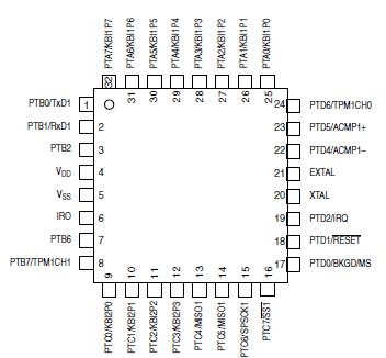
• 32-pin low-profile quad flat package (LQFP)
• 44-pin low-profile quad flat package (LQFP)
System Protection
• Optional computer operating properly (COP) reset
• Low-voltage detection with reset or interrupt
• Illegal opcode detection with reset
• Illegal address detection with reset (some devices don't have illegal addresses)
• 48-pin quad flat package (QFN)
• 39 general-purpose input/output (I/O) pins, depending on package selection
Pinout Specifications
Absolute maximum ratings are stress ratings only, and functional operation at the maxima is not uaranteed. Stress beyond the limits specified in Table A-1 may affect device reliability or cause ermanent damage to the device. For functional operating conditions, refer to the remaining tables in this ection.
This device contains circuitry protecting against damage due to high static voltage or electrical fields;however, it is advised that normal precautions be taken to avoid application of any voltages higher than aximum-rated voltages to this high-impedance circuit. Reliability of operation is enhanced if unused nputs are tied to an appropriate logic voltage level (for instance, either VSS or VDD) or the programmable ull-up resistor associated with the pin is enabled.
|
Rating |
Symbol |
Value |
Unit |
| Supply voltage |
VDD |
0.3 to +3.8 |
V |
| Maximum current into VDD |
IDD |
120 |
mA |
| Digital input voltage |
VIn |
0.3 to VDD + 0.3 |
V |
Instantaneous maximum current
Single pin limit (applies to all port pins)1,2,3 |
ID |
±25 |
mA |
| Storage temperature range |
Tstg |
55 to 150 |
°C |
1. Input must be current limited to the value specified. To determine the value of the required urrent-limiting resistor, calculate resistance values for positive (VDD) and negative (VSS) clamp oltages, then use the larger of the two resistance values.
2. All functional non-supply pins are internally clamped to VSS and VDD.
3. Power supply must maintain regulation within operating VDD range during instantaneous and perating maximum current conditions. If positive injection current (VIn > VDD) is greater than DD, the injection current may flow out of VDD and could result in external power supply going ut of regulation. Ensure external VDD load will shunt current greater than maximum injection urrent. This will be the greatest risk when the MCU is not consuming power. Examples are: if o system clock is present, or if the clock rate is very low (which would reduce overall power onsumption).
DescriptionAll TPM functions of MC9S08RC16are associated with a main 16-bit counter that allows flexible selection of the clock ource and prescale divisor. A 16-bit modulo register also is associated with the main 16-bit counter in the PM. Each TPM channel is optionally associated with an MCU pin and a maskable interrupt function.
The TPM has center-aligned PWM capabilities controlled by the CPWMS control bit in TPM1SC. When PWMS is set to 1, timer counter TPM1CNT changes to an up-/down-counter and all channels in the ssociated TPM act as center-aligned PWM channels. When CPWMS = MC9S08RC16 0, each channel can independently be configured to operate in input capture, output compare, or buffered edge-aligned PWM ode.
The following sections describe the main 16-bit counter and each of the timer operating modes of MC9S08RC16 (input apture, output compare, edge-aligned PWM, and center-aligned PWM). Because details of pin operation nd interrupt activity depend on the operating mode, these topics are covered in the associated mode ections.

 MC9S08RC16 Data Sheet


