Features: • 8-Bit HCS08 Central Processor Unit (CPU)
Up to 20 MHz CPU at 3.6 V to 1.8 V across temperature range of
40°C to 85°C
HC08 instruction set with added BGND instruction
Support for up to 32 interrupt/reset sources
• On-Chip Memory
Flash read/program/erase over full operating voltage and temperature
Random-Access memory (RAM)
Security circuitry to prevent unauthorized access to RAM and flash contents
• Power-Saving Modes
Two low power stop modes
Reduced power wait mode
Low power run and wait modes allow peripherals to run while voltage regulator is in standby
Peripheral clock gating register can disable clocks to unused modules, thereby reducing currents
Very low power external oscillator that can be used in stop2 or stop3 modes to provide accurate clock source to real time counter
6 s typical wake-up time from stop3 mode
• Clock Source Options
Oscillator (XOSC) - Loop-Control Pierce oscillator; crystal or ceramic resonator range of 31.25 kHz to 38.4 kHz or 1 MHz to 16 MHz
Internal Clock Source (ICS) - Internal clock source module containing a frequency-locked-loop (FLL) controlled by internal or external reference; precision trimming of internal reference allows 0.2% resolution and 2% deviation over temperature and voltage; supporting bus frequencies from 1 MHz to 10 MHz
• System Protection
Watchdog computer operating properly (COP) reset with option to run from dedicated 1 kHz internal clock source or bus clock
Low-Voltage warning with interrupt
Low-Voltage detection with reset or interrupt
Illegal opcode detection with reset
Illegal address detection with reset
Flash block protection
• Development Support
Single-Wire background debug interface
Breakpoint capability to allow single breakpoint setting during in-circuit debugging (plus two more breakpoints in on-chip debug module)
On-Chip in-circuit emulator (ICE) debug module containing two comparators and nine trigger modes; eight deep FIFO for storing change-of-flow addresses and event-only data; debug module supports both tag and force breakpoints
• Peripherals
ADC - 10-channel, 12-bit resolution; 2.5 s conversion time;automatic compare function; 1.7 mV/°C temperature sensor; internal bandgap reference channel; operation in stop3; fully
functional from 3.6 V to 1.8 V
ACMPx - Two analog comparators with selectable interrupt on rising, falling, or either edge of comparator output; compare option to fixed internal bandgap reference voltage; outputs can be optionally routed to TPM module; operation in stop3
SCI - Full-Duplex non-return to zero (NRZ); LIN master extended break generation; LIN slave extended break detection; wake-up on active edge
SPI - Full-Duplex or single-wire bidirectional; double-buffered transmit and receive; master or slave mode; MSB-first or LSB-first shifting
IIC - Up to 100 kbps with maximum bus loading; multi-master operation; programmable slave address; interrupt driven byte-by-byte data transfer; supporting broadcast mode and 10-bit addressing
TPMx - Two 3-channel (TPM1 and TPM2); selectable input capture, output compare, or buffered edge- or center-aligned PWM on each channel
RTC - (Real-time counter) 8-bit modulus counter with binary or decimal based prescaler; external clock source for precise time base, time-of-day, calendar or task scheduling functions; free running on-chip low power oscillator (1 kHz) for cyclic wake-up without external components; runs in all MCU modes
• Input/Output
26 GPIOs, one output-only pin and one input-only pin
Eight KBI interrupts with selectable polarity
Hysteresis and configurable pullup device on all input pins;configurable slew rate and drive strength on all output pins.
• Package Options
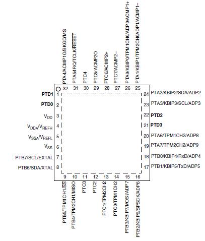
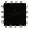
32-pin LQFP, 28-pin SOIC, 20-pin SOIC, 16-pin PDIP,16-pin TSSOP
Pinout Specifications
|
Rating |
Symbol |
Value |
Unit |
| Supply voltage |
VDD |
0.3 to +3.8 |
V |
| Maximum current into VDD |
IDD |
120 |
mA |
| Digital input voltage |
VIn |
0.3 to VDD + 0.3 |
V |
Instantaneous maximum current
Single pin limit (applies to all port pins)1,2,3 |
ID |
±25 |
mA |
| Storage temperature range |
Tstg |
55 to 150 |
°C |
1 Input must be current limited to the value specified. To determine the value of the required current-limiting resistor, calculate resistance values for positive (VDD) and negative (VSS) clamp voltages, then use the larger of the two resistance values.
2 All functional non-supply pins, except for PTA5 are internally clamped to VSS and VDD.
3 Power supply must maintain regulation within operating VDD range during instantaneous and operating maximum current conditions. If positive injection current (VIn > VDD) is greater than IDD, the injection current may flow out of VDD and could result in external power supply going out of regulation. Ensure external VDD load will shunt current greater than maximum injection current. This will be the greatest risk when the MCU is not consuming power. Examples are: if no system clock is present, or if the clock rate is very low (which would reduce overall power consumption).

 MC9S08QE8 Data Sheet


