MC9S08GT

Features: Features have been organized to reflect:• Standard features of the HCS08 Family• Features of the MC9S08GB/GT MCU1.2.1 Standard Features of the HCS08 Family• 40-MHz HCS08 CPU (central processor unit)• HC08 instruction set with added BGND instruction• Backgrou...

product image

MC9S08GT Picture
SeekIC No. : 004417386 Detail

MC9S08GT: Features: Features have been organized to reflect:• Standard features of the HCS08 Family• Features of the MC9S08GB/GT MCU1.2.1 Standard Features of the HCS08 Family• 40-MHz HCS08 ...

floor Price/Ceiling Price

Part Number:
MC9S08GT
Supply Ability:
5000

Price Break

  • Qty
  • 1~5000
  • Unit Price
  • Negotiable
  • Processing time
  • 15 Days
Total Cost: $ 0.00

SeekIC Buyer Protection PLUS - newly updated for 2013!

  • Escrow Protection.
  • Guaranteed refunds.
  • Secure payments.
  • Learn more >>

Month Sales

268 Transactions

Rating

evaluate  (4.8 stars)

Upload time: 2024/11/27

Payment Methods

All payment methods are secure and covered by SeekIC Buyer Protection PLUS.

Notice: When you place an order, your payment is made to SeekIC and not to your seller. SeekIC only pays the seller after confirming you have received your order. We will also never share your payment details with your seller.
Product Details

Description


Features:

Features have been organized to reflect:
• Standard features of the HCS08 Family
• Features of the MC9S08GB/GT MCU
1.2.1 Standard Features of the HCS08 Family
• 40-MHz HCS08 CPU (central processor unit)
• HC08 instruction set with added BGND instruction
• Background debugging system (see also the Development Support section)
• Breakpoint capability to allow single breakpoint setting during in-circuit debugging (plus two more breakpoints in on-chip debug module)
• Debug module containing two comparators and nine trigger modes. Eight deep FIFO for storing change-of-flow addresses and event-only data. Debug module supports both tag and force breakpoints.
• Support for up to 32 interrupt/reset sources
• Power-saving modes: wait plus three stops
• System protection features:
Optional computer operating properly (COP) reset
Low-voltage detection with reset or interrupt
Illegal opcode detection with reset
Illegal address detection with reset (some devices don't have illegal addresses)
1.2.2 Features of MC9S08GB/GT Series of MCUs
• On-chip in-circuit programmable FLASH memory with block protection and security options (see Table 1-1 for device specific information)
• On-chip random-access memory (RAM) (see Table 1-1 for device specific information)
• 8-channel, 10-bit analog-to-digital converter (ATD)
• Two serial communications interface modules (SCI)
• Serial peripheral interface module (SPI)
• Clock source options include crystal, resonator, external clock or internally generated clock with precision NVM trimming
• Inter-integrated circuit bus module to operate up to 100 kbps (IIC)
• One 3-channel and one 5-channel 16-bit timer/pulse width modulator (TPM) modules with selectable input capture, output compare, and edge-aligned PWM capability on each channel. Each timer module may be configured for buffered, centered PWM (CPWM) on all channels (TPMx).
• 8-pin keyboard interrupt module (KBI)
• 16 high-current pins (limited by package dissipation)
• Software selectable pullups on ports when used as input. Selection is on an individual port bit basis. During output mode, pullups are disengaged.
• Internal pullup on RESET and IRQ pin to reduce customer system cost
• Up to 56 general-purpose input/output (I/O) pins, depending on package selection
• 64-pin low-profile quad flat package (LQFP) - MC9S08GBxx
• 48-pin quad flat package, no lead (QFN) - MC9S08GTxx
• 44-pin quad flat package (QFP) - MC9S08GTxx
• 42-pin shrink dual in-line package (SDIP) - MC9S08GTxx


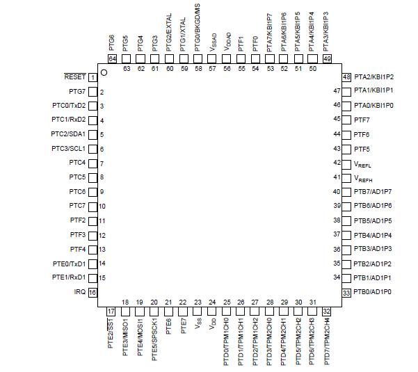
Pinout

  Connection Diagram


Specifications

Rating
Symbol
Value
Unit
Supply voltage
VDD
0.3 to +3.8
V
Maximum current into VDD
IDD
120
mA
Digital input voltage
VIn
0.3 to VDD + 0.3
V
Instantaneous maximum current
Single pin limit (applies to all port pins)(1), (2), (3)
ID
± 25
mA
Storage temperature range
Tstg
55 to 150
°C
NOTES:
1. Input must be current limited to the value specified. To determine the value of the required current-limiting resistor, calculate resistance values for positive (VDD) and negative (VSS) clamp voltages, then use the larger of the two resistance values.
2. All functional non-supply pins are internally clamped to VSS and VDD.
3. Power supply must maintain regulation within operating VDD range during instantaneous and operating maximum current conditions. If positive injection current (VIn > VDD) is greater than IDD, the injection current may flow out of VDD and could result in external power supply going out of regulation. Ensure external VDD load will shunt current greater than maximum injection current. This will be the greatest risk when the MCU is not consuming power. Examples are: if no system clock is present, or if the clock rate is very low which would reduce overall power consumption.


Customers Who Bought This Item Also Bought

Margin,quality,low-cost products with low minimum orders. Secure your online payments with SeekIC Buyer Protection.
Prototyping Products
DE1
Programmers, Development Systems
Power Supplies - External/Internal (Off-Board)
Optoelectronics
Discrete Semiconductor Products
View more