Features: • Up to 1000 program/erase cycles at typical voltage and temperature
• Security feature for Flash
• Uses a single pin for background debug serial communications
• Non-intrusive of user memory resources; BDC registers are not located in the memory map
• SYNC command to determine target communications rate
• Non-intrusive commands allow access to memory resources while CPU is running user code without stopping applications
• Active background mode commands for CPU register access
• GO and TRACE1 commands
• BACKGROUND command can wake CPU from wait or stop modes
• BDC_RESET command allows host to reset MCU without using a reset pin
• One hardware address breakpoint built into BDC
• RS08 clock source runs in stop mode if BDM enabled to allow debugging when CPU is in stop mode
• COP watchdog suspended while in active background mode
Pinout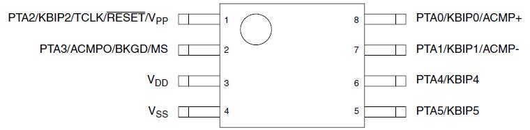 Specifications
Absolute maximum ratings are stress ratings only, and functional operation at the maxima is not guaranteed. Stress beyond the limits specified in Table A-1 may affect device reliability or cause permanent damage to the device. For functional operating conditions, refer to the remaining tables in this chapter.
This device contains circuitry protecting against damage due to high static voltage or electrical fields;however, it is advised that normal precautions be taken to avoid application of any voltages higher than maximum-rated voltages to this high-impedance circuit. Reliability of operation is enhanced if unused inputs are tied to an appropriate logic voltage level (for instance, either VSS or VDD) or the programmable pull-up resistor associated with the
|
Symbol |
Parameter |
Value |
Unit |
|
VDD |
Supply voltage |
0.3 to +5.8 |
V |
|
IDD |
Maximum current into VDD |
120 |
mA |
|
VIn |
Digital input voltage |
0.3 to VDD + 0.3 |
V |
|
ID |
Instantaneous maximum current
Single pin limit (applies to all port pins)1, 2, 3 |
±25 |
mA |
|
TSTG |
Storage temperature range |
-55 ~+150 |
°C |
1 Input must be current limited to the value specified. To determine the value of the required current-limiting resistor, calculate resistance values for positive (VDD) and negative (VSS) clamp voltages, then use the larger of the two resistance values.
2 All functional non-supply pins are internally clamped to VSS and VDD except the RESET/VPP pin which is internally clamped to VSS only.
3 Power supply must maintain regulation within operating VDD range during instantaneous and operating maximum current conditions. If positive injection current (VIn > VDD) is greater than IDD, the injection current may flow out of VDD and could result in external power supply going out of regulation. Ensure external VDD load will shunt current greater than maximum injection current. This will be the greatest risk when the MCU is not consuming power. Examples are: if no system clock is present, or if the clock rate is very low which would reduce overall power consumption.
DescriptionThe analog comparator MC9RS08KA1 can be used to compare two analog input voltages applied to ACMP+ and ACMP; or MC9RS08KA1 can be used to compare an analog input voltage applied to ACMP with an internal bandgap reference voltage. ACBGS is used to select between the bandgap reference voltage or the ACMP+ pin as the input to the non-inverting input of the analog comparator.
The comparator output MC9RS08KA1 is high when the non-inverting input is greater than the inverting input, and MC9RS08KA1 is low when the non-inverting input is less than the inverting input. ACMOD is used to select the condition which will cause ACF to be set. ACF can be set on a rising edge of the comparator output of MC9RS08KA1, a falling edge of the comparator output, or either a rising or a falling edge (toggle). The comparator output can be read directly through ACO. The comparator output can also be driven onto the ACMPO pin using ACOPE

 MC9RS08KA1 Data Sheet