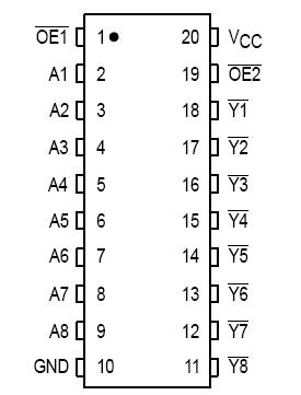
Features: • High Speed: tPD = 3.7ns (Typ) at VCC = 5V• Low Power Dissipation: ICC = 4mA (Max) at TA = 25°C• TTLCompatible Inputs: VIL = 0.8V; VIH = 2.0V• Power Down Protection Provided on Inputs• Balanced Propagation Delays• Designed for 2V to 5.5V Operating Ran...
MC74VHCT540A: Features: • High Speed: tPD = 3.7ns (Typ) at VCC = 5V• Low Power Dissipation: ICC = 4mA (Max) at TA = 25°C• TTLCompatible Inputs: VIL = 0.8V; VIH = 2.0V• Power Down Protectio...
SeekIC Buyer Protection PLUS - newly updated for 2013!
268 Transactions
All payment methods are secure and covered by SeekIC Buyer Protection PLUS.
Features: Operating range: 38 to 47 Gb/s (min.) (note)Signal regeneration with full-rate clock sig...
Symbol | Parameter | Value | Unit |
VCC | DC Supply Voltage (Referenced to GND) | 0.5 to +7.0 | V |
VIN | DC Input Voltage (Referenced to GND) | 0.5 to +7.0 | V |
Vout | DC Output Voltage (Referenced to GND) | 0.5toVCC + 0.5 |
V |
Iik | DC Input Current, per Pin | -20 | mA |
Iok | DC Output Sink/Source Current, per Pin | ±20 | mA |
lout | DC Output Source/Sink Current | ±25 | |
ICC | DC VCC or GND Current per Output Pin | ±75 | mA |
pd | Power dissipation in still | 500 400 |
|
Tstg | Storage Temperature | 65 to +150 | °C |
The MC74VHCT540A is an advanced high speed CMOS inverting octal bus buffer fabricated with silicon gate CMOS technology. It achieves high speed operation similar to equivalent Bipolar Schottky TTL while maintaining CMOS low power dissipation.
The MC74VHCT540A features inputs and outputs on opposite sides of the package and two ANDed activelow output enables. When either OE1 or OE2 are high, the terminal outputs are in the high impedance state. The VHCT MC74VHCT540A inputs are compatible with TTL levels. This device can be used as a level converter for interfacing 3.3V to 5.0V, because it has full 5V CMOS level output swings.
The VHCT540A input and output (when disabled) structures provide protection when voltages between 0V and 5.5V are applied, regardless of the supply voltage. These input and output structures help prevent device destruction caused by supply voltage input/output voltage mismatch, battery backup, hot insertion, etc.
The internal circuit of MC74VHCT540A is composed of three stages, including a buffer output which provides high noise immunity and stable output. The inputs tolerate voltages up to 7V, allowing the interface of 5V systems to 3V systems.