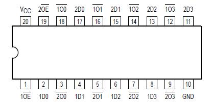
Features: • Designed for 2.7 to 3.6V VCC Operation• 5V Tolerant - Interface Capability With 5V TTL Logic• Supports Live Insertion and Withdrawal• IOFF Specification Guarantees High Impedance When VCC = 0V• LVTTL Compatible• LVCMOS Compatible• 24mA Balanced...
MC74LCX240: Features: • Designed for 2.7 to 3.6V VCC Operation• 5V Tolerant - Interface Capability With 5V TTL Logic• Supports Live Insertion and Withdrawal• IOFF Specification Guarantee...
SeekIC Buyer Protection PLUS - newly updated for 2013!
268 Transactions
All payment methods are secure and covered by SeekIC Buyer Protection PLUS.
Features: Operating range: 38 to 47 Gb/s (min.) (note)Signal regeneration with full-rate clock sig...
Symbol | Parameter | Value | Condition | Unit |
VCC | DC Supply Voltage | 0.5 to +7.0 | V | |
VI | DC Input Voltage | 0.5 VI VCC + 0.5V | V | |
VO | DC Output Voltage | 0.5 VO VCC + 0.5 0.5 VO VCC + 0.5 |
Output in 3State Note 1. |
V |
IIK | DC Input Diode Current | 50 | VI < GND | mA |
IOK | DC Output Diode Current | 50 +50 |
VO < GND VO > VCC |
mA |
IO | DC Output Source/Sink Current | ±50 | mA | |
ICC | DC Supply Current | ±100 | mA | |
IGND | DC Ground Current | ±100 | mA | |
TSTG | Storage Temperature Range | 65 to +150 | °C |
* Absolute maximum continuous ratings are those values beyond which damage to the device may occur. Exposure to these conditions or conditions beyond those indicated may adversely affect device reliability. Functional operation under absolutemaximumrated conditions is not implied.
The MC74LCX240 is a high performance, inverting octal buffer operating from a 2.7 to 3.6V supply. High impedance TTL compatible inputs significantly reduce current loading to input drivers while TTL compatible outputs offer improved switching noise performance. A VI specification of 5.5V allows MC74LCX240 inputs to be safely driven from 5V devices. The MC74LCX240 is suitable for memory address driving and all TTL level bus oriented transceiver applications. Current drive capability is 24mA at the outputs. The Output Enable (OE) input, when HIGH, disables the outputs by placing them in a HIGH Z condition.