MC74HC4851A

Features: • Injection Current CrossCoupling Less than 1mV/mA (See Figure 9)• Pin Compatible to HC405X and MC1405XB Devices• Power Supply Range (VCC GND) = 2.0 to 6.0 V• In Compliance With the Requirements of JEDEC Standard No. 7A• Chip Complexity: 154 FETs or 36 Equi...

product image

MC74HC4851A Picture
SeekIC No. : 004416992 Detail

MC74HC4851A: Features: • Injection Current CrossCoupling Less than 1mV/mA (See Figure 9)• Pin Compatible to HC405X and MC1405XB Devices• Power Supply Range (VCC GND) = 2.0 to 6.0 V• In C...

floor Price/Ceiling Price

Part Number:
MC74HC4851A
Supply Ability:
5000

Price Break

  • Qty
  • 1~5000
  • Unit Price
  • Negotiable
  • Processing time
  • 15 Days
Total Cost: $ 0.00

SeekIC Buyer Protection PLUS - newly updated for 2013!

  • Escrow Protection.
  • Guaranteed refunds.
  • Secure payments.
  • Learn more >>

Month Sales

268 Transactions

Rating

evaluate  (4.8 stars)

Upload time: 2024/11/27

Payment Methods

All payment methods are secure and covered by SeekIC Buyer Protection PLUS.

Notice: When you place an order, your payment is made to SeekIC and not to your seller. SeekIC only pays the seller after confirming you have received your order. We will also never share your payment details with your seller.
Product Details

Description


Features:

• Injection Current CrossCoupling Less than 1mV/mA (See Figure 9)
• Pin Compatible to HC405X and MC1405XB Devices
• Power Supply Range (VCC GND) = 2.0 to 6.0 V
• In Compliance With the Requirements of JEDEC Standard No. 7A
• Chip Complexity: 154 FETs or 36 Equivalent Gates


• Injection Current CrossCoupling Less than 1mV/mA (See Figure 9)
• Pin Compatible to HC405X and MC1405XB Devices
• Power Supply Range (VCC GND) = 2.0 to 6.0 V
• In Compliance With the Requirements of JEDEC Standard No. 7A
• Chip Complexity: 154 FETs or 36 Equivalent Gates


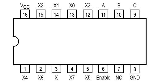
Pinout

  Connection Diagram

  Connection Diagram


Specifications

Symbol Parameter Value Unit
vcc DC Supply Voltage (Referenced to GND) 0.5 to +7.0 V
VIN DC Input Voltage (Referenced to GND) 0.5 to VCC + 0.5 V
VOUT DC Output Voltage (Referenced to GND) 0.5 to VCC + 0.5 V
LIN DC Input Current, per Pin ±20 mA
IOUT DC Onput Current, per Pin ±35 mA
ICC DC Supply Current Per Supply Pin ±75 mA
PD Power dissipation in still air piastic DIP
SOIC package
750
500
450
mW
TSTG Storage Temperature 65 to +150 °C
TL Lead Temperature, 1 mm from Case for 10 Seconds
(Plastic DIP or SOIC Package)
260
°C
* Maximum Ratings are those values beyond which damage to the device may occur.
Functional operation should be restricted to the Recommended Operating Conditions.
†Derating - Plastic DIP: 10 mW/C from 65 to 125C
Ceramic DIP: 10 mW/C from 100 to 125C
SOIC Package: 7 mW/C from 65 to 125C
For high frequency or heavy load considerations, see Chapter 2 of the Motorola HighSpeed CMOS Data Book (DL129/D).


Description

MC74HC4851A are pin compatible to standard HC405x and MC1405xB analog mux/demux devices, but feature injection current effect control. This makes them especially suited for usage in automotive applications where voltages in excess of normal logic voltage are common.

The injection current effect control allows signals at disabled analog input channels to exceed the supply voltage range without affecting the signal of the enabled analog channel. This eliminates the need for external diode/ resistor networks typically used to keep the analog channel signals within the supply voltage range.

MC74HC4851A utilize low power silicon gate CMOS technology. The Channel Select and Enable inputs are compatible with standard CMOS outputs.


Customers Who Bought This Item Also Bought

Margin,quality,low-cost products with low minimum orders. Secure your online payments with SeekIC Buyer Protection.
Memory Cards, Modules
Isolators
Semiconductor Modules
Cables, Wires - Management
Test Equipment
Soldering, Desoldering, Rework Products
View more