Maximum Input Frequency
:
Minimum Input Frequency
:
Output Frequency Range
:
Number of Circuits
: 1
Type
: PLL
Supply Voltage - Max
: 6 V
Supply Voltage - Min
: 2 V
Maximum Operating Temperature
: + 125 C
Package / Case
: PDIP-16
Minimum Operating Temperature
: - 55 C
Packaging
: UPAK
Features: • Output Drive Capability: 10 LSTTL Loads
• Low Power Consumption Characteristic of CMOS Devices
• Operating Speeds Similar to LSTTL
• Wide Operating Voltage Range: 3.0 to 6.0 V
• Low Input Current: 1.0 mA Maximum (except SIGIN and COMPIN)
• In Compliance with the Requirements Defined by JEDEC Standard No. 7A
• Low Quiescent Current: 80 mA Maximum (VCO disabled)
• High Noise Immunity Characteristic of CMOS Devices
• Diode Protection on all Inputs
• Chip Complexity: 279 FETs or 70 Equivalent GatesPinout Specifications
| Symbol |
Parameter |
Value |
Unit |
| vcc |
DC Supply Voltage (Referenced to GND) |
0.5 to +7.0 |
V |
| VIN |
DC Input Voltage (Referenced to GND) |
0.5 to VCC + 0.5 |
V |
| VOUT |
DC Output Voltage (Referenced to GND) |
0.5 to VCC + 0.5 |
V |
| LIN |
DC Input Current, per Pin |
±20 |
mA |
| IOUT |
DC Onput Current, per Pin |
±25 |
mA |
| ICC |
DC Supply Current Per Supply Pin |
±50 |
mA |
| PD |
Power dissipation in still air piastic DIP
SOIC package
|
750
500
|
mW |
| TSTG |
Storage Temperature |
65 to +150 |
°C |
| TL |
Lead Temperature, 1 mm from Case for 10 Seconds
(Plastic DIP or SOIC Package) |
260
|
°C |
* Maximum Ratings are those values beyond which damage to the device may occur.
Functional operation should be restricted to the Recommended Operating Conditions.
†Derating - Plastic DIP: 10 mW/ from 65 to 125
Ceramic DIP: 10 mW/ from 100 to 125
SOIC Package: 7 mW/ from 65to 125
For high frequency or heavy load considerations, see Chapter 2 of the Motorola HighSpeed CMOS Data Book (DL129/D).DescriptionThe MC74HC4046A is similar in function to the MC14046 Metal gate CMOS device. The device inputs are compatible with standard CMOS outputs; with pullup resistors, they are compatible with LSTTL outputs.
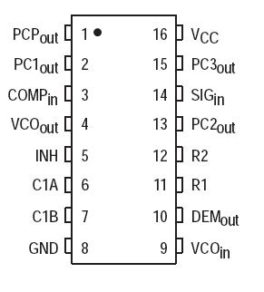
The HC4046A phaselocked loop contains three phase comparators, a voltagecontrolled oscillator (VCO) and unity gain opamp DEMOUT. The comparators have two common signal inputs, COMPIN, and SIGIN. Input SIGIN and COMPIN can be used directly coupled to large voltage signals, or indirectly coupled (with a series capacitor to small voltage signals). The selfbias circuit of MC74HC4046AN adjusts small voltage signals in the linear region of the amplifier. Phase comparator 1 (an exclusive OR gate) provides a digital error signal PC1OUT and maintains 90 degrees phase shift at the center frequency between SIGIN and COMPIN signals (both at 50% duty cycle). Phase comparator 2 (with leadingedge sensing logic) provides digital error signals PC2OUT and PCPOUT and maintains a 0 degree phase shift between SIGIN and COMPIN signals (duty cycle is immaterial). The linear VCO produces an output signal VCOOUT whose frequency is determined by the voltage of input VCOIN signal and the capacitor and resistors connected to pins C1A, C1B, R1 and R2. The unity gain opamp output DEMOUT with an external resistor is used where the VCOIN signal is needed but no loading can be tolerated. The inhibit
nput, when high, disables the VCO and all opamps to minimize standby power consumption.
Applications of MC74HC4046AN include FM and FSK modulation and demodulation, frequency synthesis and multiplication, frequency discrimination, tone decoding, data synchronization and conditioning, voltagetofrequency conversion and motor speed control.
Parameters: | Technical/Catalog Information | MC74HC4046AN |
| Vendor | ON Semiconductor |
| Category | Integrated Circuits (ICs) |
| Type | Phase Lock Loop (PLL) |
| Voltage - Supply | 3 V ~ 6 V |
| Number of Outputs | 6 |
| Input | - |
| Output | - |
| Frequency-Max | 13MHz |
| Package / Case | 16-DIP |
| Packaging | Tube |
| Operating Temperature | -55°C ~ 125°C |
| Lead Free Status | Contains Lead |
| RoHS Status | RoHS Non-Compliant |
| Other Names | MC74HC4046AN
MC74HC4046AN
MC74HC4046ANOS ND
MC74HC4046ANOSND
MC74HC4046ANOS
|

 MC74HC4046AN Data Sheet


