Features: • Output Drive Capability: 10 LSTTL Loads
• Outputs Directly Interface to CMOS, NMOS, and TTL
• Operating Voltage Range: 2 to 6 V
• Low Input Current: 1 A
• High Noise Immunity Characteristic of CMOS Devices
• In Compliance With JEDEC Standard No. 7A Requirements
• Chip Complexity: 398 FETs or 99.5 Equivalent Gates
ApplicationA 60Hz sinewave obtained through a 1.0 Megohm resistor connected directly to a standard 120 Vac power line is applied to the input of the MC54/74HC14A, Schmitt-trigger inverter. The HC14A squaresup the input waveform and feeds the HC4040A. Selecting outputs Q5, Q10, Q11, and Q12 causes a reset every 3600 clocks. The HC20 decodes the counter outputs, produces a single (narrow) output pulse, and resets the binary counter. The resulting output frequency is 1.0 pulse/minute.
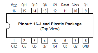
Pinout Specifications
|
Symbol |
Parameter |
Value |
Unit |
|
VCC |
DC Supply Voltage (Referenced to GND) |
0.5 to + 7.0 |
V |
|
Vin |
DC Input Voltage (Referenced to GND) |
0.5 to VCC + 0.5 |
V |
|
Vout |
DC Output Voltage (Referenced to GND) |
0.5 to VCC + 0.5 |
V |
|
Iin |
DC Input Current, per Pin |
± 20 |
mA |
|
Iout |
DC Output Current, per Pin |
± 25 |
mA |
|
ICC |
DC Supply Current, VCC and GND Pins |
± 50 |
mA |
|
PD |
Power Dissipation in Still Air, Plastic or Ceramic DIP
SOIC Package
TSSOP Package |
750
500
450 |
mW |
|
Tstg |
Storage Temperature Range |
65 to + 150 |
|
|
TL |
Lead Temperature, 1 mm from Case for 10 Seconds
Plastic DIP, SOIC or TSSOP Package
Ceramic DIP
|
260
300 |
|
* Maximum Ratings are those values beyond which damage to the device may occur.Functional operation should
be restricted to the Recommended Operating Conditions.
†Derating - Plastic DIP: 10 mW/ from 65° to 125
Ceramic DIP: 10 mW/ from 100° to 125
SOIC Package: 7 mW/ from 65° to 125
TSSOP Package: 6.1 mW/ from 65° to 125
For high frequency or heavy load considerations, see Chapter 2 of the Motorola HighSpeed CMOS Data Book (DL129/D).
This device contains protection circuitry to guard against damage due to high static voltages or electric fields. However, precautions must be taken to avoid applications of any voltage higher than maximum rated
voltages to this highimpedance circuit. For proper operation, Vin and Vout should be constrained to the
range GND (Vin or Vout) VCC. Unused inputs must always be tied to an appropriate logic voltage
level (e.g., either GND or VCC). Unused outputs must be left open.DescriptionThe MC54/74C4040A is identical in pinout to the standard CMOS MC14040. The device inputs are compatible with standard CMOS outputs; with pullup resistors, they are compatible with LSTTL outputs.
MC74HC4040A consists of 12 masterslave flipflops. The output of each flipflop feeds the next and the frequency at each output is half of that of the preceding one. The state counter advances on the negativegoing edge of the Clock input. Reset is asynchronous and activehigh.
State changes of the Q outputs do not occur simultaneously because of internal ripple delays. Therefore, decoded output signals of MC74HC4040A are subject to decoding spikes and may have to be gated with the Clock of the HC4040A for some designs.

 MC74HC4040A Data Sheet


