MC74ACT823

Features: • 3-State Outputs for Bus Interfacing• Broad Side Pin Configuration• ACT has TTL Compatible Inputs• High Speed Parallel Positive Edge-Triggered D-Type Flip-Flops• High Performance Bus Interface Buffering for Busses Carrying Parity• Outputs Source/Sink...

product image

MC74ACT823 Picture
SeekIC No. : 004416758 Detail

MC74ACT823: Features: • 3-State Outputs for Bus Interfacing• Broad Side Pin Configuration• ACT has TTL Compatible Inputs• High Speed Parallel Positive Edge-Triggered D-Type Flip-Flops&#...

floor Price/Ceiling Price

Part Number:
MC74ACT823
Supply Ability:
5000

Price Break

  • Qty
  • 1~5000
  • Unit Price
  • Negotiable
  • Processing time
  • 15 Days
Total Cost: $ 0.00

SeekIC Buyer Protection PLUS - newly updated for 2013!

  • Escrow Protection.
  • Guaranteed refunds.
  • Secure payments.
  • Learn more >>

Month Sales

268 Transactions

Rating

evaluate  (4.8 stars)

Upload time: 2024/11/27

Payment Methods

All payment methods are secure and covered by SeekIC Buyer Protection PLUS.

Notice: When you place an order, your payment is made to SeekIC and not to your seller. SeekIC only pays the seller after confirming you have received your order. We will also never share your payment details with your seller.
Product Details

Description


Features:

• 3-State Outputs for Bus Interfacing
• Broad Side Pin Configuration
• ACT has TTL Compatible Inputs
• High Speed Parallel Positive Edge-Triggered D-Type Flip-Flops
• High Performance Bus Interface Buffering for Busses Carrying Parity
• Outputs Source/Sink 24 mA


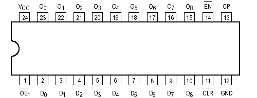
Pinout

  Connection Diagram


Specifications

Symbol
Parameter
Value
Unit
VCC
DC Supply Voltage (Referenced to GND)
0.5 to +7.0
V
Vin
DC Input Voltage (Referenced to GND)
0.5 to VCC +0.5
V
Vout
DC Output Voltage (Referenced to GND)
0.5 to VCC +0.5
V
Iin
DC Input Current, per Pin
±20
mA
Iout
DC Output Sink/Source Current, per Pin
±50
mA
ICC
DC VCC or GND Current per Output Pin
±50
mA
Tstg
Storage Temperature  Range
65 to +150
* Maximum Ratings are those values beyond which damage to the device may occur. Functional operation
   should be restricted to the Recommended Operating Conditions.


Description

The MC74AC/ACT823 consists of nine D-type edge-triggered flip-flops. MC74ACT823 has 3-state outputs for bus systems, organized in a broadside pinning. In addition to the clock and output enabled pins, the buffered clock (CP) and buffered Output Enable (OE) are common to all flip-flips. The flip-flops MC74ACT823 will store the state of their individual D inputs that meet the setup and hold time requirements on the LOW-to-HIGH CP transition. With OE LOW, the contents of the flip-flops are available at the outputs. When OE is HIGH, the outputs go to the high impedance state.

Operation of the OEinput MC74ACT823 does not affect the state of the flip-flops. The MC74AC/ACT823 has Clear (CLR) and Clock Enable (EN) pins. These devices are ideal for parity bus interfacing in high performance systems.

When CLR is LOW, and OE is LOW, the outputs are LOW. When CLR is HIGH, data can be entered into the flip-flops. When EN MC74ACT823 is LOW, data on the inputs is transferred to the outputs on the LOW-to-HIGH clock transition. When EN is HIGH, the outputs do not change state, regardless of the data or clock input transitions.


Customers Who Bought This Item Also Bought

Margin,quality,low-cost products with low minimum orders. Secure your online payments with SeekIC Buyer Protection.
Memory Cards, Modules
Boxes, Enclosures, Racks
Soldering, Desoldering, Rework Products
Discrete Semiconductor Products
Line Protection, Backups
Prototyping Products
DE1
View more