MC74ACT259

Features: • Serial-to-Parallel Conversion• Eight Bits of Storage with Output of Each Bit Available• Random (Addressable) Data Entry• Active High Demultiplexing or Decoding Capability• Easily Expandable• Common ClearThe MC74AC259/74ACT259 has four modes of operat...

product image

MC74ACT259 Picture
SeekIC No. : 004416729 Detail

MC74ACT259: Features: • Serial-to-Parallel Conversion• Eight Bits of Storage with Output of Each Bit Available• Random (Addressable) Data Entry• Active High Demultiplexing or Decoding Ca...

floor Price/Ceiling Price

Part Number:
MC74ACT259
Supply Ability:
5000

Price Break

  • Qty
  • 1~5000
  • Unit Price
  • Negotiable
  • Processing time
  • 15 Days
Total Cost: $ 0.00

SeekIC Buyer Protection PLUS - newly updated for 2013!

  • Escrow Protection.
  • Guaranteed refunds.
  • Secure payments.
  • Learn more >>

Month Sales

268 Transactions

Rating

evaluate  (4.8 stars)

Upload time: 2024/11/27

Payment Methods

All payment methods are secure and covered by SeekIC Buyer Protection PLUS.

Notice: When you place an order, your payment is made to SeekIC and not to your seller. SeekIC only pays the seller after confirming you have received your order. We will also never share your payment details with your seller.
Product Details

Description


Features:

• Serial-to-Parallel Conversion
• Eight Bits of Storage with Output of Each Bit Available
• Random (Addressable) Data Entry
• Active High Demultiplexing or Decoding Capability
• Easily Expandable
• Common Clear

The MC74AC259/74ACT259 has four modes of operation as shown in the Mode Selection Table. In the addressable latch mode, data on the Data line (D) is written into the addressed latch. The addressed latch will follow the data input with all nonaddressed latches remaining in their previous states in the memory mode. All latches remain in their previous state and are unaffected by the Data or Address inputs.

In the one-of-eight decoding or demultiplexing mode, the addressed output will follow the state of the D input with all other outputs in the LOW state. In the clear mode all outputs are LOW and unaffected by the address and data inputs. When operating the MC74AC/ACT259 as an addressable latch, changing more than one bit of the address could impose a transient wrong address. Therefore, this should only be done while in the memory mode. The Mode Select Function Table summarizes the operations of the MC74AC/ACT259.


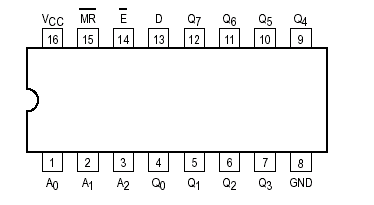
Pinout

  Connection Diagram


Specifications

Symbol
Parameter
Value
Unit
VCC
DC Supply Voltage (Referenced to GND)
0.5 to +7.0
V
Vin
DC Input Voltage (Referenced to GND)
0.5 to VCC +0.5
V
Vout
DC Output Voltage (Referenced to GND)
0.5 to VCC +0.5
V
Iin
DC Input Current, per Pin
±20
mA
Iout
DC Output Sink/Source Current, per Pin
±50
mA
ICC
DC VCC or GND Current per Output Pin
±50
mA
Tstg
Storage Temperature
65 to +150
* Maximum Ratings are those values beyond which damage to the device may occur. Functional operation
   should be restricted to the Recommended Operating Conditions.


Description

The MC74AC259/74ACT259 is a high-speed 8-bit addressable latch designed for general purpose storage applications in digital systems. MC74ACT259 is a multifunctional device capable of storing single line data in eight addressable latches, and also a 1-of-8 decoder and demultiplexer with active HIGH outputs. The device also incorporates an active LOW Common Clear for resetting all latches, as well as an active LOW Enable. It is functionally identical to the ALS259 8-bit addressable latch.


Customers Who Bought This Item Also Bought

Margin,quality,low-cost products with low minimum orders. Secure your online payments with SeekIC Buyer Protection.
Optical Inspection Equipment
Power Supplies - External/Internal (Off-Board)
Motors, Solenoids, Driver Boards/Modules
Potentiometers, Variable Resistors
LED Products
Memory Cards, Modules
View more