MC7445

Features: Major features of the MPC7455 are as follows:• High-performance, superscalar microprocessor - As many as four instructions can be fetched from the instruction cache at a time - As many as three instructions can be dispatched to the issue queues at a time - As many as 12 instruction...

product image

MC7445 Picture
SeekIC No. : 004416616 Detail

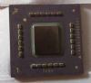
MC7445: Features: Major features of the MPC7455 are as follows:• High-performance, superscalar microprocessor - As many as four instructions can be fetched from the instruction cache at a time - As ma...

floor Price/Ceiling Price

Part Number:
MC7445
Supply Ability:
5000

Price Break

  • Qty
  • 1~5000
  • Unit Price
  • Negotiable
  • Processing time
  • 15 Days
Total Cost: $ 0.00

SeekIC Buyer Protection PLUS - newly updated for 2013!

  • Escrow Protection.
  • Guaranteed refunds.
  • Secure payments.
  • Learn more >>

Month Sales

268 Transactions

Rating

evaluate  (4.8 stars)

Upload time: 2024/5/9

Payment Methods

All payment methods are secure and covered by SeekIC Buyer Protection PLUS.

Notice: When you place an order, your payment is made to SeekIC and not to your seller. SeekIC only pays the seller after confirming you have received your order. We will also never share your payment details with your seller.
Product Details

Description


Features:

Major features of the MPC7455 are as follows:
• High-performance, superscalar microprocessor
  - As many as four instructions can be fetched from the instruction cache at a time
  - As many as three instructions can be dispatched to the issue queues at a time
  - As many as 12 instructions can be in the instruction queue (IQ)
  - As many as 16 instructions can be at some stage of execution simultaneously
  - Single-cycle execution for most instructions
  - One instruction per clock cycle throughput for most instructions
  - Seven-stage pipeline control

• Eleven independent execution units and three register files
  - Branch processing unit (BPU) features static and dynamic branch prediction
     128-entry (32-set, four-way set-associative) branch target instruction cache (BTIC), a cache of
         branch  instructions that have been encountered in branch/loop code sequences. If a target instruction 
         is in the BTIC, it is fetched into the instruction queue a cycle sooner than it can be made available from
         the instruction cache. Typically, a fetch that hits the BTIC provides the first four instructionsin the target
         stream.
     2048-entry branch history table (BHT) with two bits per entry for four levels ofprediction-not-taken,
         strongly not-taken, taken, and strongly taken
     Up to three outstanding speculative branches
     Branch instructions that do not update the count register (CTR) or link register (LR) are oftenremoved from
         the instruction stream.
     Eight-entry link register stack to predict the target address of Branch Conditional to Link Register
         (bclr) instructions
  - Four integer units (IUs) that share 32 GPRs for integer operands
     Three identical IUs (IU1a, IU1b, and IU1c) can execute all integer instructions except multiply,divide,
         and move to/from special-purpose register instructions
     IU2 executes miscellaneous instructions including the CR logical operations, integer multiplication and
        division instructions, and move to/from special-purpose register instructions
  - Five-stage FPU and a 32-entry FPR file
     Fully IEEE 754-1985-compliant FPU for both single- and double-precision operations
     Supports non-IEEE mode for time-critical operations
     Hardware support for denormalized numbers
     Thirty-two 64-bit FPRs for single- or double-precision operands
  - Four vector units and 32-entry vector register file (VRs)
     Vector permute unit (VPU)
     Vector integer unit 1 (VIU1) handles short-latency AltiVec™ integer instructions, such as vector add
         instructions (vaddsbs, vaddshs, and vaddsws, for example)
     Vector integer unit 2 (VIU2) handles longer-latency AltiVec integer instructions, such as vectormultiply
         add instructions (vmhaddshs, vmhraddshs, and vmladduhm, for example)
     Vector floating-point unit (VFPU)
  - Three-stage load/store unit (LSU)
     Supports integer, floating-point, and vector instruction load/store traffic
     Four-entry vector touch queue (VTQ) supports all four architected AltiVec data stream operations
     Three-cycle GPR and AltiVec load latency (byte, half-word, word, vector) with one-cycle throughput
     Four-cycle FPR load latency (single, double) with one-cycle throughput
     No additional delay for misaligned access within double-word boundary
     Dedicated adder calculates effective addresses (EAs)
     Supports store gathering
     Performs alignment, normalization, and precision conversion for floating-point data
     Executes cache control and TLB instructions
     Performs alignment, zero padding, and sign extension for integer data
     Supports hits under misses (multiple outstanding misses)
     Supports both big- and little-endian modes, including misaligned little-endian accesses

• Three issue queues FIQ, VIQ, and GIQ can accept as many as one, two, and three instructions, respectively,
    in a cycle. Instruction dispatch requires the following:
  - Instructions can be dispatched only from the three lowest IQ entries-IQ0, IQ1, and IQ2
  - A maximum of three instructions can be dispatched to the issue queues per clock cycle
  - Space must be available in the CQ for an instruction to dispatch (this includes instructions that areassigned
      a space in the CQ but not in an issue queue)

• Rename buffers
  - 16 GPR rename buffers
  - 16 FPR rename buffers
  - 16 VR rename buffers

• Dispatch unit
  - Decode/dispatch stage fully decodes each instruction

• Completion unit
  - The completion unit retires an instruction from the 16-entry completion queue (CQ) when allinstructions
      ahead of it have been completed, the instruction has finished execution, and no exceptions are pending.
  - Guarantees sequential programming model (precise exception model)
  - Monitors all dispatched instructions and retires them in order
  - Tracks unresolved branches and flushes instructions after a mispredicted branch
  - Retires as many as three instructions per clock cycle

• Separate on-chip L1 instruction and data caches (Harvard architecture)
  - 32-Kbyte, eight-way set-associative instruction and data caches
  - Pseudo least-recently-used (PLRU) replacement algorithm
  - 32-byte (eight-word) L1 cache block
  - Physically indexed/physical tags
  - Cache write-back or write-through operation programmable on a per-page or per-block basis
  - Instruction cache can provide four instructions per clock cycle; data cache can provide four words per clock cycle
  - Caches can be disabled in software
  - Caches can be locked in software
  - MESI data cache coherency maintained in hardware
  - Separate copy of data cache tags for efficient snooping
  - Parity support on cache and tags
  - No snooping of instruction cache except for icbi instruction
  - Data cache supports AltiVec LRU and transient instructions
  - Critical double- and/or quad-word forwarding is performed as needed. Critical quad-word forwarding is
      used for AltiVec loads and instruction fetches. Other accesses use critical double-word forwarding.

• Level 2 (L2) cache interface
  - On-chip, 256-Kbyte, eight-way set-associative unified instruction and data cache
  - Fully pipelined to provide 32 bytes per clock cycle to the L1 caches
  - A total nine-cycle load latency for an L1 data cache miss that hits in L2
  - PLRU replacement algorithm
  - Cache write-back or write-through operation programmable on a per-page or per-block basis
  - 64-byte, two-sectored line size
  - Parity support on cache

• Level 3 (L3) cache interface (not implemented on MPC7445)
  - Provides critical double-word forwarding to the requesting unit
  - Internal L3 cache controller and tags
  - External data SRAMs
  - Support for 1- and 2-Mbyte L3 caches
  - Cache write-back or write-through operation programmable on a per-page or per-block basis
  - 64-byte (1M) or 128-byte (2M) sectored line size
  - Private memory capability for half (1-Mbyte minimum) or all of the L3 SRAM space
  - Supports MSUG2 dual data rate (DDR) synchronous Burst SRAMs, PB2 pipelined synchronous Burst SRAMs, 
      and pipelined (register-register) late write synchronous Burst SRAMs
  - Supports parity on cache and tags
  - Configurable core-to-L3 frequency divisors
  - 64-bit external L3 data bus sustains 64 bits per L3 clock cycle

• Separate memory management units (MMUs) for instructions and data
  - 52-bit virtual address; 32- or 36-bit physical address
  - Address translation for 4-Kbyte pages, variable-sized blocks, and 256-Mbyte segments
  - Memory programmable as write-back/write-through, caching-inhibited/caching-allowed, and memory
     coherency  enforced/memory coherency not enforced on a page or block basis
  - Separate IBATs and DBATs (eight each) also defined as SPRs
  - Separate instruction and data translation lookaside buffers (TLBs)
     Both TLBs are 128-entry, two-way set-associative, and use LRU replacement algorithm
     TLBs are hardware- or software-reloadable (that is, on a TLB miss a page table search is performed
         in hardware or by system software)

• Efficient data flow
  - Although the VR/LSU interface is 128 bits, the L1/L2/L3 bus interface allows up to 256 bits
  - The L1 data cache is fully pipelined to provide 128 bits/cycle to or from the VRs
  - L2 cache is fully pipelined to provide 256 bits per processor clock cycle to the L1 cache
  - As many as eight outstanding, out-of-order, cache misses are allowed between the L1 data cache and
      L2/L3 bus
  - As many as 16 out-of-order transactions can be present on the MPX bus
  - Store merging for multiple store misses to the same line. Only coherency action taken (address-only)
      for store misses merged to all 32 bytes of a cache block (no data tenure needed).
  - Three-entry finished store queue and five-entry completed store queue between the LSU and the L1
     data cache
  - Separate additional queues for efficient buffering of outbound data (such as castouts and write through
      stores) from the L1 data cache and L2 cache

• Multiprocessing support features include the following:
  - Hardware-enforced, MESI cache coherency protocols for data cache
  - Load/store with reservation instruction pair for atomic memory references, semaphores, and other 
     multiprocessor operations

• Power and thermal management
  - 1.3-V processor core
  - The following three power-saving modes are available to the system:
      Nap-Instruction fetching is halted. Only those clocks for the time base, decrementer, and JTAG logic
         remain running. The part goes into the doze state to snoop memory operations on the bus and then
         back to nap using a QREQ /QACK processor-system handshake protocol.
     Sleep-Power consumption is further reduced by disabling bus snooping, leaving only the PLL in a locked
         and running state. All internal functional units are disabled.
     Deep sleep-When the part is in the sleep state, the system can disable the PLL. The system can then
        disable the SYSCLK source for greater system power savings. Power-on reset procedures for restarting 
        and relocking the PLL must be followed on exiting the deep sleep state.
  - Thermal management facility provides software-controllable thermal management. Thermal management
      is performed through the use of three supervisor-level registers and an MPC7455-specific thermal
      management  exception.
  - Instruction cache throttling provides control of instruction fetching to limit power consumption

• Performance monitor can be used to help debug system designs and improve software efficiency
• In-system testability and debugging features through JTAG boundary-scan capability

• Testability
  - LSSD scan design
  - IEEE 1149.1 JTAG interface
  - Array built-in self test (ABIST)-factory test only

• Reliability and serviceability
  - Parity checking on system bus and L3 cache bus
  - Parity checking on the L2 and L3 cache tag arrays


Description

The MPC7455 and MPC7445 are implementations of the PowerPC™ microprocessor family of reduced instruction set
computer (RISC) microprocessors. MC7445 is primarily concerned with the MPC7455; however, unless otherwise noted, all information here also applies to the MPC7445. This document describes pertinent electrical and physical characteristics of the MPC7455. For functional characteristics of MC7445, refer to the MPC7450 RISC Microprocessor Family User's Manual. To locate any published updates for this document, refer to the website at http://www.freescale.com.


Customers Who Bought This Item Also Bought

Margin,quality,low-cost products with low minimum orders. Secure your online payments with SeekIC Buyer Protection.
Prototyping Products
DE1
Batteries, Chargers, Holders
Transformers
Circuit Protection
Power Supplies - External/Internal (Off-Board)
Computers, Office - Components, Accessories
View more