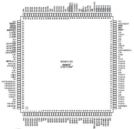
Features: The following paragraphs highlight capabilities of each of the MCU modules. Each module is discussed separately in a subsequent section of this manual.PinoutSpecifications Num Rating Symbol Value Unit 1 Supply Voltage1, 2, 3 VDD 0.3 to + 6.5 V 2 I...
MC68HC916Y3: Features: The following paragraphs highlight capabilities of each of the MCU modules. Each module is discussed separately in a subsequent section of this manual.PinoutSpecifications Num Ra...
SeekIC Buyer Protection PLUS - newly updated for 2013!
268 Transactions
All payment methods are secure and covered by SeekIC Buyer Protection PLUS.
Num |
Rating |
Symbol |
Value |
Unit |
1 |
Supply Voltage1, 2, 3 |
VDD |
0.3 to + 6.5 |
V |
2 |
Input Voltage1, 2, 3, 4, 5, 7 |
Vin |
0.3 to + 6.5 |
V |
3 |
Instantaneous Maximum Current Single pin limit (applies to all pins)1, 3, 5, 6 |
ID |
25 |
mA |
4 |
Operating Maximum Current Digital Input Disruptive Current3, 5, 6, 7, 8 VNEGCLAMP 0.3 V VPOSCLAMP VDD + 0.3 V |
IID |
500 to + 500 |
A |
5 |
Flash EEPROM Program/Erase Supply Voltage9, 10 |
VFPE |
(VDD 0.35) to +12.6 |
V |
6 |
Operating Temperature Range C Suffix V Suffix M Suffix |
TA |
TL to TH 40 to + 85 40 to + 105 40 to + 125 |
°C |
7 |
Storage Temperature Range |
Tstg |
55 to + 150 |
°C |
NOTES:
1. Permanent damage can occur if maximum ratings are exceeded. Exposure to voltages or currents in excess of recommended values affects device reliability. Device modules may not operate normally while being exposed to electrical extremes.
2. Although sections of the device contain circuitry to protect against damage from high static voltages or electrical fields, take normal precautions to avoid exposure to voltages higher than maximum-rated voltages.
3. This parameter is periodically sampled rather than 100% tested.
4. All pins except TSC.
5. Input must be current limited to the value specified. To determine the value of the required current-limiting resistor, calculate resistance values for positive and negative clamp voltages, then use the larger of the two values.
6. Power supply must maintain regulation within operating VDD range during instantaneous and operating maximum current conditions.
7. All functional non-supply pins are internally clamped to VSS for transitions below VSS. All functional pins except EXTAL, TSC, and XFC are internally clamped to VDD for transitions below VDD.
8. Total input current for all digital input-only and all digital input/output pins must not exceed 10 mA. Exceeding this limit can cause disruption of normal operation.
9. VFPE must not be raised to programming level while VDD is below specified minimum value. VFPE must not
be reduced below minimum specified value while VDD is applied.
10. Flash EEPROM modules can be damaged by power-on and power-off VFPE transients. Maximum power-on overshoot tolerance is 13.5 V for periods of less than 30 ns.