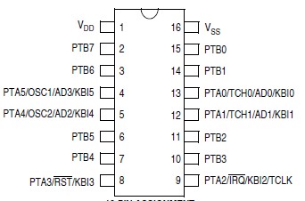
Features: Features include:
• High-performance M68HC08 CPU core
• Fully upward-compatible object code with M68HC05 Family
• 5-V and 3-V operating voltages (VDD)
• 8-MHz internal bus operation at 5 V, 4-MHz at 3 V
• Trimmable internal oscillator
Software selectable 1 MHz, 2 MHz, or 3.2 MHz internal bus operation
8-bit trim capability
± 25% untrimmed
Trimmable to approximately 0.4%(1)
• Software selectable crystal oscillator range, 32100 kHz, 18 MHz, and 832 MHz
• Software configurable input clock from either internal or external source
• Auto wakeup from STOP capability using dedicated internal 32-kHz RC or bus clock source
• On-chip in-application programmable FLASH memory
Internal program/erase voltage generation
Monitor ROM containing user callable program/erase routines
FLASH security(2)Pinout SpecificationsMaximum ratings are the extreme limits to which the microcontroller unit (MCU) can be exposed without permanently damaging it.
NOTE This device is not guaranteed to operate properly at the maximum ratings. Refer to 18.5 5-V DC Electrical Characteristics and 18.8 3-V DC Electrical Characteristics for guaranteed operating onditions.
|
Characteristic(1) |
Symbol |
Value |
Unit |
|
Supply voltage |
VDD |
0.3 to +6.0 |
V |
|
Input voltage |
VIN |
VSS 0.3 to VDD +0.3 |
V |
|
Mode entry voltage, IRQ pin |
VTST |
VSS 0.3 to +9.1 |
V |
|
Maximum current per pin excluding
PTA0PTA5, VDD, and VSS |
I |
±15 |
mA |
|
Maximum current for pins PTA0PTA5 |
IPTA0-IPTA5 |
±25 |
mA |
|
Storage temperature |
TSTG |
55 to +150 |
°C |
|
Maximum current out of VSS |
IMVSS |
100 |
mA |
|
Maximum current into VDD |
IMVDD |
100 |
mA |
1. Voltages references to VSS.
NOTE This device contains circuitry to protect the inputs against damage due to high static voltages or electric fields; however, it is advised that normal precautions be taken to avoid application of any voltage higher than maximum-rated voltages to this high-impedance circuit. For proper operation, it is recommended that VIN and VOUT be constrained to the range VSS (VIN or VOUT) VDD. Reliability of operation is enhanced if unused inputs are connected to an appropriate logic voltage level (for example, either VSS or VDD.)DescriptionThe MC68HC908QY8 features are as follows:
• On-chip random-access memory (RAM)
• Enhanced serial communications interface (ESCI) module
• Serial peripheral interface (SPI) module
• 4-channel, 16-bit timer interface (TIM) module
• 10-channel, 10-bit analog-to-digital converter (ADC) with internal bandgap reference channel (ADC10)
• Up to 13 bidirectional input/output (I/O) lines and one input only:
Six shared with KBI
Ten shared with ADC
Four shared with TIM
Two shared with ESCI
Four shared with SPI
One input only shared with IRQ
High current sink/source capability on all port pins
Selectable pullups on all ports, selectable on an individual bit basis
Three-state ability on all port pins
• 6-bit keyboard interrupt with wakeup feature (KBI)
Programmable for rising/falling or high/low level detect
• Low-voltage inhibit (LVI) module features:
Software selectable trip point
• System protection features:
Computer operating properly (COP) watchdog
Low-voltage detection with reset
Illegal opcode detection with reset
Illegal address detection with reset
• External asynchronous interrupt pin with internal pullup (IRQ) shared with general-purpose input pin
• Master asynchronous reset pin with internal pullup (RST) shared with general-purpose input/output (I/O) pin
• Memory mapped I/O registers
• Power saving stop and wait modes
• MC68HC908QB8, MC68HC908QB4 and MC68HC908QY8 are available in these packages:
16-pin plastic dual in-line package (PDIP)
16-pin small outline integrated circuit (SOIC) package
16-pin thin shrink small outline packages (TSSOP)

 MC68HC908QY8 Data Sheet


