MC68HC908QL4

Features: Features include:• High-performance M68HC08 CPU core• Fully upward-compatible object code with M68HC05 Family• 5-V and 3.3-V operating voltages (VDD)• 8-MHz internal bus operation at 5 V, 4-MHz at 3.3 V• Software configurable input clock from either internal...

product image

MC68HC908QL4 Picture
SeekIC No. : 004416546 Detail

MC68HC908QL4: Features: Features include:• High-performance M68HC08 CPU core• Fully upward-compatible object code with M68HC05 Family• 5-V and 3.3-V operating voltages (VDD)• 8-MHz interna...

floor Price/Ceiling Price

Part Number:
MC68HC908QL4
Supply Ability:
5000

Price Break

  • Qty
  • 1~5000
  • Unit Price
  • Negotiable
  • Processing time
  • 15 Days
Total Cost: $ 0.00

SeekIC Buyer Protection PLUS - newly updated for 2013!

  • Escrow Protection.
  • Guaranteed refunds.
  • Secure payments.
  • Learn more >>

Month Sales

268 Transactions

Rating

evaluate  (4.8 stars)

Upload time: 2024/11/27

Payment Methods

All payment methods are secure and covered by SeekIC Buyer Protection PLUS.

Notice: When you place an order, your payment is made to SeekIC and not to your seller. SeekIC only pays the seller after confirming you have received your order. We will also never share your payment details with your seller.
Product Details

Description


Features:

Features include:
• High-performance M68HC08 CPU core
• Fully upward-compatible object code with M68HC05 Family
• 5-V and 3.3-V operating voltages (VDD)
• 8-MHz internal bus operation at 5 V, 4-MHz at 3.3 V
• Software configurable input clock from either internal or external source

• Trimmable internal oscillator
   Selectable 1 MHz, 2 MHz, or 3.2MHz or 6.4 MHz internal bus operation
   8-bit trim capability
   Trimmable to approximately 0.4%(1)
   ± 25% untrimmed

• Software selectable crystal oscillator range, 32100 kHz, 18 MHz, and 832 MHz
• Auto wakeup from STOP capability using dedicated internal 32-kHz RC or bus clock source

• On-chip in-application programmable FLASH memory
   Internal program/erase voltage generation
  Monitor ROM containing user callable program/erase routines
   FLASH security(2)

• On-chip random-access memory (RAM)
• Slave LIN interface controller (SLIC) module
  Full LIN messaging buffering of Identifier and 8 data bytes
  Automatic baud rate and LIN message frame synchronization:No prior programming of bit rate required, 
     120 kbps LIN bus speed operation All LIN messages will be received (no message loss due to
     synchronization process) Input clock tolerance as high as ±50%, allowing internal oscillator to remain
     untrimmed Incoming break symbols allowed to be 10 to 20 bit times without message loss Supports
     automatic software trimming of internal oscillator using LIN synchronization data
  Automatic processing and verification of LIN SYNCH BREAK and SYNCH BYTE
  Automatic checksum calculation and verification with error reporting
  Maximum of 2 interrupts per LIN message frame
  Full LIN error checking and reporting
  High-speed LIN capability up to 83.33 kbps to 120.00 kbps
  Switchable UART-like byte transfer mode for processing bytes one at a time without LIN message
      framing constraints
   Configurable digital receive filter

• 2-channel, 16-bit timer interface module (TIM) with external clock source input
• 6-channel, 10-bit analog-to-digital converter (ADC) with internal bandgap reference channel (ADC10)
• 6-bit keyboard interrupt with wakeup feature (KBI)
  Programmable for rising/falling or high/low level detect
  Software selectable to use internal or external pullup/pulldown device

• External asynchronous interrupt pin with internal pullup (IRQ)
• Master asynchronous reset pin with internal pullup (RST)

• 13 bidirectional input/output (I/O) lines and one input only:
  Six shared with keyboard interrupt function
  Six shared with ADC10
  Two shared with TIM
  Two shared with SLIC
  One shared with reset
  One input only shared with external interrupt (IRQ)
  High current sink/source capability
  Selectable pullups on all ports (pullup/down on port A), selectable on an individual bit basis
  Three-state ability on all port pins

• Low-voltage inhibit (LVI) module features:
  Software selectable trip point in CONFIG register

• System protection features:
  Computer operating properly (COP) watchdog
  Low-voltage detection with reset
  Illegal opcode detection with reset
  Illegal address detection with reset

• Power-on reset
• Memory mapped I/O registers
• Power saving stop and wait modes

• Available packages:
  16-pin small outline integrated circuit (SOIC) package
  16-pin thin shrink small outline package (TSSOP)
Features of the CPU08 include the following:
• Enhanced HC05 programming model
• Extensive loop control functions
• 16 addressing modes (eight more than the HC05)
• 16-bit index register and stack pointer
• Memory-to-memory data transfers
• Fast 8 * 8 multiply instruction
• Fast 16/8 divide instruction
• Binary-coded decimal (BCD) instructions
• Optimization for controller applications
• Efficient C language support


Application

www.freescale.com


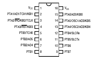
Pinout

  Connection Diagram


Description

The MC68HC908QL4 is a member of the low-cost, high-performance M68HC08 Family of 8-bit microcontroller units (MCUs). All MCUs MC68HC908QL4 in the family use the enhanced M68HC08 central processor unit (CPU08) and are available with a variety of modules, memory sizes and types, and package types.


Customers Who Bought This Item Also Bought

Margin,quality,low-cost products with low minimum orders. Secure your online payments with SeekIC Buyer Protection.
Audio Products
Computers, Office - Components, Accessories
Power Supplies - Board Mount
Undefined Category
Semiconductor Modules
View more